1 PCB board production process - substrate use
2 PCB board production process - metal coating
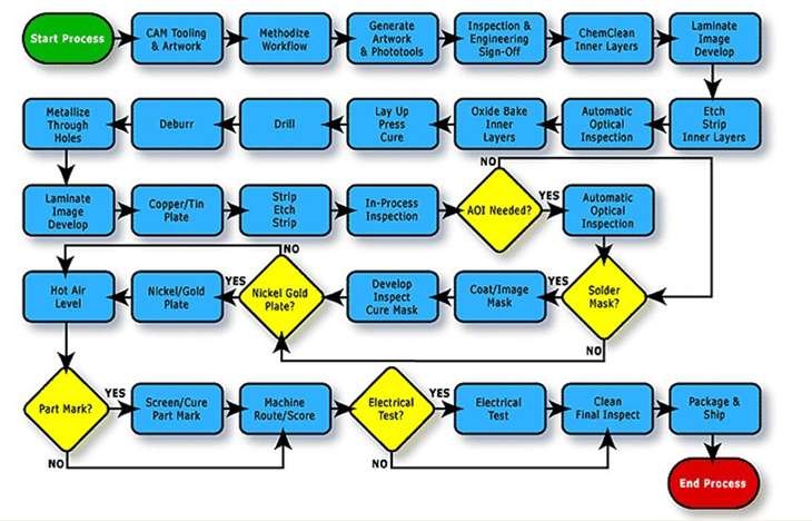
3 PCB board production process - basic production
4 PCB board production process - functional test
5 PCB board production process - technical level
6 PCB board production process - automatic exploration
7 PCB board production process - boundary scanPCB board production process - substrate processing
The substrate is generally classified by the insulating portion of the substrate. Common raw materials are electric wood, fiberglass, and various plastic plates. Manufacturers of PCBs generally use an insulating part composed of glass fiber, non-woven material, and resin, and then press it into a "prepreg" with epoxy resin and copper foil.
PCB board production process - metal coating
In addition to the wiring on the substrate, the metal coating is where the substrate wiring is soldered to the electronic components. In addition, because of the different prices of different metals, it directly affects the cost of production. In addition, each metal has different solderability, contact properties, resistance values, etc., which will directly affect the performance of the component.
Commonly used metal coatings are: copper, tin (usually 5 to 15 μm thick), lead-tin alloy (or tin-copper alloy, ie solder, thickness usually 5 to 25 μm, tin content about 63%), gold (generally only Will be plated in the interface), silver (generally only plated on the interface, or alloyed with silver as a whole).
PCB board production process - basic production
According to different technologies, it can be divided into two major categories of processes.
Subtraction method
Subtractive is the removal of unwanted areas on a blank circuit board (ie, a circuit board covered with a complete piece of metal foil) using chemicals or machinery. The remaining convenience is the required circuit.
Screen printing: The pre-designed circuit diagram is made into a mesh screen. The unnecessary circuit parts on the screen are covered with wax or impervious material. Then the screen mask is placed on the blank circuit board and then on the wire. The protective agent that will not be corroded on the oil on the net will put the circuit board into the corrosive liquid. The part not covered by the protective agent will be eroded away, and finally the protective agent will be cleaned.
Photosensitive plate: The pre-designed circuit diagram is made on a light-transmissive film mask (the simplest method is to use the printer to print the slide). Similarly, the required part should be printed as an opaque color, and then in the blank line. The board is coated with photographic pigment, and the prepared film mask is placed on the circuit board to illuminate the glare for a few minutes. After removing the mask, the pattern on the circuit board is displayed with the developer, and finally, as with the screen printing method. Corrode the circuit.
Marking: Use the milling machine or laser engraving machine to directly remove unwanted parts of the blank line.Addition method
Additive, now commonly used on a substrate pre-plated with thin copper, covered with photoresist (D / F), exposed to ultraviolet light and then developed, exposed where needed, and then used to plate the circuit board On the official line, the copper thickness is thickened to the required specifications, and then an anti-etching resist-metal thin tin is applied, and finally the photoresist is removed (this process is called film removal), and then the copper foil under the photoresist is applied. The layer is etched away.
Laminated method
The laminate method is one of the methods for producing a multilayer printed circuit board. The outer layer is wrapped after the inner layer is made, and the outer layer is treated by subtraction or addition. By repeating the operation of the lamination method, it is possible to obtain a multilayer multilayer printed circuit board which is a sequential lamination method.
1. Inner layer production
2. Layered (ie, the action of bonding different layers)
3. The completion of the layering (subtracting the outer metal foil film of the method; addition method)
4. Drilling
Panel plating
1. Full block PCB plating
2. Add a barrier layer to the surface where it is to be retained (resist)
3. Etching
4. Remove the barrier layer
Pattern plating
1. Add a barrier layer to the surface where it is not to be retained.
2. Electroplating required surface to a certain thickness
3. Remove the barrier layer
4. Etching to unwanted metal foil film disappears
Complete addition method
1. Add a barrier layer to the place where the conductor is not needed.
2. Composition line with electroless copper
Partial addition method
1. Cover the entire PCB with electroless copper
2. Add a barrier layer to the place where the conductor is not needed.
3. Electrolytic copper plating
4. Remove the barrier layer
5. Etching until the original electroless copper disappears under the barrier layer
PCB board production process - functional test
More intensive PCBs, higher bus speeds, and analog RF circuits present unprecedented challenges for testing. Functional testing in this environment requires careful design, well-thought-out testing methods, and appropriate tools to provide credible Test Results.
Think about where the product will be made. For example, we assume that the test engineer is in California, USA, and the product is manufactured in Thailand. Test engineers will consider the product to require expensive automated fixtures because of the high price of the plant in California, requiring as few testers as possible, and the use of automated fixtures to reduce the need to hire high-tech, high-paying operators. But in Thailand, these two problems do not exist.
PCB board production process - technical level
In high-density UUTs, if calibration or diagnostics are required, it is likely to be manually probed because the needle bed contact is limited and the test is faster (using the probe to test the UUT can quickly acquire data instead of feeding back information to the edge) For reasons such as connectors, it is required that the operator probe the test points on the UUT. Wherever you are, make sure that the test points are clearly marked.
Probe types and general operators should also be aware that issues to consider include:
Is the probe larger than the test point? Does the probe have the risk of shorting several test points and damaging the UUT? Is there an electric shock hazard to the operator?
Can every operator quickly find a test point and check it? Is the test point large and easy to identify?
How long does it take for the operator to press the probe on the test point to get an accurate reading? If the time is too long, there will be some trouble in the small test area. If the operator's hand will slide because the test time is too long, it is recommended to expand the test area to avoid this problem.
After considering the above issues, the test engineer should re-evaluate the type of test probe, modify the test file to better identify the location of the test point, or even change the requirements for the operator.
PCB board production process - automatic exploration
In some cases, automatic probing is required, such as when the PCB is difficult to manually explore, or when the skill level of the operator is limited, so that the test speed is greatly reduced, then an automated method should be considered.
Automated probing eliminates human error, reduces the likelihood of shorts at several test points, and speeds up test operations. However, be aware that there may be some limitations to automated profiling, depending on the vendor's design, including:
UUT size
Number of sync probes
How close are the two test points?
Test probe positioning accuracy
Can the system perform two-sided detection of the UUT?
How fast is the probe moved to the next test point?
What is the actual separation required by the probe system? (Generally speaking, it is bigger than the offline functional test system)
Automatic probing usually does not require needle bed clamps to contact other test points, and generally it is slower than the production line, so two steps may be required: if the detector is used only for diagnostics, consider using a traditional functional test system on the production line. The detector is placed on the side of the production line as a diagnostic system; if the purpose of the detector is UUT calibration, the only real solution is to use multiple systems, knowing that this is much faster than manual operation.
How to integrate into the production line is also a key issue that must be studied. Is there still room on the production line? Can the system be connected to the conveyor belt? Fortunately, many new probing systems are compatible with the SMEMA standard, so they can work in an online environment.
PCB board production process - boundary scan
This technique should be discussed as early as the product design phase because it requires specialized components to perform this task. In UUTs dominated by digital circuits, devices with IEEE1194 (Boundary Scan) support can be purchased so that most diagnostic problems can be solved with little or no probing. Boundary scanning reduces the overall functionality of the UUT because it increases the area of each compatible device (4 to 5 pins per chip and some lines), so the principle of choosing this technology is the cost. It should be possible to improve the diagnosis. It should be remembered that boundary scan can be used to program flash memory and PLD devices on the UUT, which further increases the reason for choosing this test method.
How to deal with a limited design?
If the UUT design has been completed and determined, the selection is limited. Of course, you can also request modifications in the next revision or new product, but process improvement always takes a certain amount of time, and you still have to deal with the current situation.