Contents
1 PCB board production process - circuit design2 PCB layout design should pay attention to matters
3 PCB board production problems
PCB board production process - circuit design
The design of the printed circuit board is based on the circuit schematic and realizes the functions required by the circuit user. Printed circuit board design mainly refers to the layout design, which requires internal electronic components, metal wiring, through-hole and external connection layout, electromagnetic protection, heat dissipation, crosstalk and other factors. Excellent circuit design can save production costs and achieve good circuit performance and heat dissipation. Simple layouts can be implemented manually, but complex circuit designs typically require computer-aided design (CAD), and well-known design software includes OrCAD, Pads (also known as PowerPCB), Altium Designer (also known as Protel), and FreePCB. , CAM350, etc.
PCB layout design should pay attention to matters
Single panel:
This type of panel is typically used at lower cost requirements. In layout, sometimes components or jumpers are required to skip the traces of the board. If the number is too large, you should consider using a double panel.Double panel:
Dual panels may or may not use PTH. Because PTH boards are expensive, they are used when the complexity and density of the circuit is needed. In the layout, the number of wires on the component side must be kept to a minimum to ensure easy access to the required materials.
In PTH boards, plated through holes are used only for electrical connections and not for component mounting. For economic and reliability reasons, the number of holes should be kept to a minimum.
To choose a single panel or a double panel, it is important to consider the surface area of the component (C), which is a suitable constant ratio to the total area (S) of the printed circuit board. The installation is useful. It is worth noting that the US "usually refers to the area of one side of the panel.
Design inspections, the following checklists cover all aspects of the design cycle, and for special: applications should add additional items.
1) Is the circuit analyzed? Is there a basic unit for smoothing the signal circuit?2) Does the circuit allow for short or isolated key leads?
3) Is the place that must be shielded effectively shielded?
4) Make full use of the basic grid graphics?
5) Is the size of the printed board the best size?
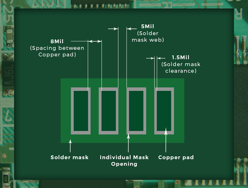
6) Is the selected wire width and spacing as much as possible?
7) Is the preferred pad size and hole size used?
8) Is the photographic plate and sketch suitable?
9) Is the minimum number of jumpers used? Should the jumper pass through components and accessories?
10) Is the letter visible after assembly? Is the size and model correct?
11) In order to prevent blistering, does the large area of copper foil open the window?
12) Is there a tool positioning hole?