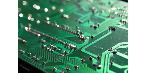
What is OSP?
OSP (Organic Solderability Preservatives) is an organic solder protection film, also known as a copper protection agent. In other words, OSP is chemically grows an organic film on the clean bare copper surface. This film has oxidation resistance, thermal shock resistance, and moisture resistance. It is used to protect the copper surface from rusting (oxidation or vulcanization, etc.) in the normal environment. However, in the subsequent high-temperature soldering, this protective film must be easily and quickly removed by the flux. This allows the exposed clean copper surface to bond instantly with the molten solder into a strong solder joint in a very short time.
In AiPCBA, we has comprehensive PCB manufacturing capabilities. Whether it is OSP, HASL, ENIG and other surface treatments, our factory can provide one-stop solutions for you. For more details, you can learn about our PCB manufacturing capabilities now!
The advantage of OSP in PCBA Process
OSP has many advantages, such as a good flat surface, and no IMC formation between the copper of the pad. Solder and copper are allowed to be directly soldered (good wettability) during soldering, and low-temperature processing technology. Low cost (can be lower than HASL) and low energy use during processing, etc.The disadvantage of OSP in PCBA Process
(1)Of course, the surface treatment of OSP in PCBA processing also has its shortcomings. For example, there are many types of actual formulations and different performances.
(2)The protective film formed by the OSP process is extremely thin and is easily scratched (or scratched), and must be handled with care.
(3)At the same time, discoloration or cracks may occur in the OSP film that has undergone multiple high-temperature soldering processes, which will affect solderability and reliability.
The note for OSP boards in the PCBA Process
(1)The PCB should be vacuum packed, and a desiccant and humidity display card should be attached. When transporting and storing, use insulation paper between PCBs with OSP to prevent friction from damaging the OSP surface.
(2) Do not directly expose to the sun, keep a good warehouse environment, relative humidity: 30~70%, temperature: 15~30 ℃, storage period is less than 6 months.
(3) When unpacking at the SMT site, you must check the vacuum packaging, desiccant, humidity display card, etc. The unqualified board is returned to the factory for reprocessing and reuse, and it goes online within 8 hours. Do not open more than one package at a time, follow the principle of production as soon as it is dismantled, or dismantle as much as you can, otherwise the exposure time is too long and it is likely to cause bad quality welding accidents.
(4) Do not stay in the furnace as soon as possible after printing (the stay should not exceed 1 hour), because the flux in the solder paste corrodes the OSP film very strongly.
(5) Maintain a good workshop environment: relative humidity 40 ~ 60%, temperature: 18 ~ 27 ℃.
(6) During the production process, avoid touching the PCB surface directly with your hands, so as not to be oxidized by sweat pollution.
(7) After the SMT single-sided patch is completed, the second-sided SMT component patch assembly must be completed within 12 hours.
(8) After completing SMT, complete the DIP hand plug-in in the shortest possible time (up to 24 hours).
(9) Wet baking OSP PCB can not be used. High temperature baking will easily make OSP discolor and deteriorate.
All PCBs in AiPCBA are produced based on UL and ISO certification standards. All our normal specification PCB are strictly obeying to IPC-A-6011/6012 Class 2 latest version and IPC-A-600 Class 2 latest version. All our production operations are strictly in accordance with international standards. As a One-Stop PCB Assembly Service provider, AiPCBA has accepted many orders for turnkey PCB assembly from all over the world. To this day, it is still well received.
PCB Assembly is one of the AiPCBA’s main activities. We are able to undertake a high-quality Printed Circuit Board Assembly at favourable prices and flexible conditions. Within PCB Assembly we utilize most of the assembly technologies: Thru-Hole axial, radial assembly, manual assembly, SMT assembly (01005-45mm x 45mm, BGA, uBGA), Reflow, Dispense technologies. Learn more About AiPCBA Turnkey PCB Assembly.
SMT solder paste stencil design requirements for OSP PCB
(1)Because the OSP is flat, it is beneficial to the formation of solder paste, and PAD cannot provide a part of the solder, so the opening should be appropriately enlarged to ensure that the solder can cover the entire pad. When the PCB was changed from sprayed tin to OSP, the stencil required reopening.
(2)When designing the stencil, try to make the solder paste cover the pad as much as possible. According to the IPC 610-D version of the PCBA solder paste quality visual inspection standard, a small portion of exposed copper on the edge of the pad can be judged to be acceptable, but the coverage rate must be at least 80% of the pad area.
(3)If the parts are not placed on the PCB for any reason, the solder paste should also cover the pad as much as possible.
(4)In order to prevent the OSP PCB from waiting too long in the SMT process to cause oxidation of the through-holes, resulting in solderability and reliability problems. Consider printing all ICT test points and DIP through-holes with solder paste at the solder paste printing station to protect the through-holes from oxidation and rust.
AiPCBA is a PCBA manufacturer which focuses on one-stop PCBA intelligent manufacturing services, using artificial intelligence and big data technology, independently developed China's first PCBA flexible intelligent manufacturing platform AiPCBA®, integrating electronic components sourcing, product prototype, trial production, volume production, to provide customers with high-quality, high-efficiency quality services.
Get the instant online Quote in AiPCBA!