1.What is Surface Finish in PCB Manufacturing?
The PCB has a copper substrate surface. Without a protective layer, the copper surface is prone to oxidation, which can lead to difficulties in soldering. Surface finish can protect the exposed copper circuits and provide a solderable surface during soldering.
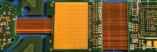
As shown in the diagram below, the surface finish is located on the outermost layer of the PCB, above the copper layers, serving as a "coating" for the copper.
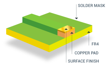
pcb surface finish
The surface finish of PCB is one of the most crucial processes in PCB manufacturing.
AiPCBA is one of the largest PCB/PCBA manufacturers in China, offering 8 types of surface finish processes, as well as various hybrid surface finish processes. At AiPCBA, we are certain to meet all your PCB manufacturing process requirements.
2.7 Types of Circuit Board Surface Finishes
· 1.Hot air solder level (HASL)
· 2.Immersion tin (ImSn)
· 3.Electroless nickel immersion gold (ENIG)
· 4.Organic solderability preservatives (OPS)
· 5.Immersion silver (ImAg)
· 6.Electroless nickel electroless palladium immersion gold (ENEPIG)
· 7.Electrolytic Nickel/Gold
· 8.Hybrid PCB Surface Finishes technology
The following is a comparison of the advantages and disadvantages of 7 types of surfacefinishes comparison.
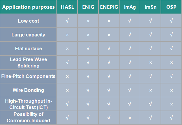
7 types of Circuit Board Surface Finishes
3.Printed Circuit Board Surface Finishes: advantages and disadvantages
- Hot air solder level (HASL)
HASL stands for Hot Air Solder Leveling, a process in which molten tin-lead solder is applied to the surface of a PCB, and then heated while compressed air is used to level and smooth the solder, creating a coating layer that is resistant to copper oxidation and exhibits good solderability.
HASL Copper Plating Example
HASL refers to the formation of copper-tin intermetallic compounds at the junction where solder and copper combine, with a thickness of approximately 1 to 2 mils.
HASL is divided into two types: one is leaded solder spray, and the other is lead-free solder spray, with lead-free being more environmentally friendly.From the surface perspective, leaded solder appears brighter, while lead-free solder looks duller.
Process Flow: Micro-etching - Preheating - Coating Flux - Tin Spraying - Cleaning
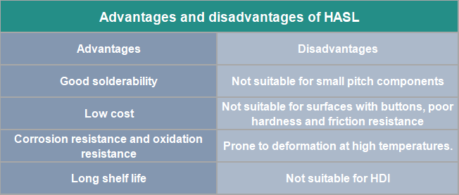
Advantages and disadvantages of HASL
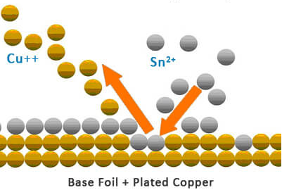
- Immersion tin (ImSn)
Simply put,ImSnis the process of depositing a layer of tin on a clean bare copper surface through a chemical oxidation-reduction reaction.This tin layer exhibits anti-oxidation, heat resistance, and moisture resistance.
After adding organic additives to the tin immersion solution, the tin layer exhibits a granular structure, overcoming the issues of tin whiskers and tin migration. Meanwhile, it also possesses good thermal stability and solderability.
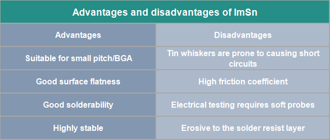
Advantages and disadvantages of ImSn
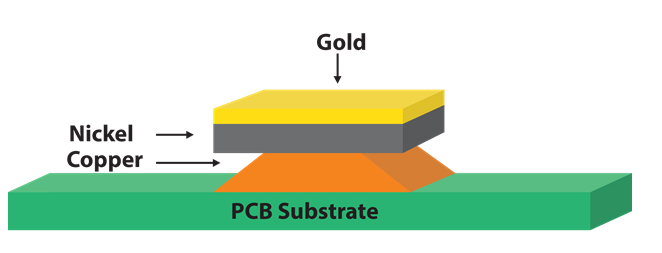
- Electroless nickel immersion gold plating (ENIG)
ENIG surface finish can meet the requirements of small pitch devices (BGA and μBGA) for surface flatness and lead-free processing on PCBs.
ENIG is a two-step process, involving the deposition of a thin layer of nickel over the copper surface, followed by a thin layer of gold. Nickel serves as a barrier for copper and acts as the actual surface to which components are soldered, while gold protects nickel during storage.
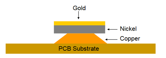
· The inner layer thickness of Ni is typically 3 to 6 μm, and the deposition thickness of the outer layer Au is generally 0.05 to 0.1 μm.
· Ni forms a barrier layer between solder and copper.
· The role of Au is to prevent oxidation of Ni during storage, thereby extending the shelf life. However, the gold-plating process also results in excellent surface flatness.
Common applications include high-density PCBs, rigid PCBs, and flexible PCBs in industries such as aerospace, military, medical, consumer electronics, and more.
Process Flow: Deacidification and Cleaning - Microetching - Pre-dip - Activation - Electroless Nickel Plating - Chemical Immersion Gold
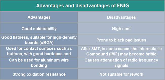
Advantages and disadvantages of ENIG
- Organic solderability preservatives (OSP)
OSP (Organic Solderability Preservatives) involves applying a very thin protective layer on exposed copper to shield it from oxidation.This film possesses characteristics such as anti-oxidation, resistance to thermal shocks, and moisture resistance. Its role is to protect the copper surface from rusting (oxidation or sulfuration, etc.) under normal environmental conditions.
In other words, OSP acts as a barrier between copper and the surrounding air.
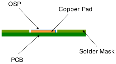
The general process for OSP includes: degreasing -> microetching -> acid cleaning -> pure water rinsing -> organic coating -> cleaning.
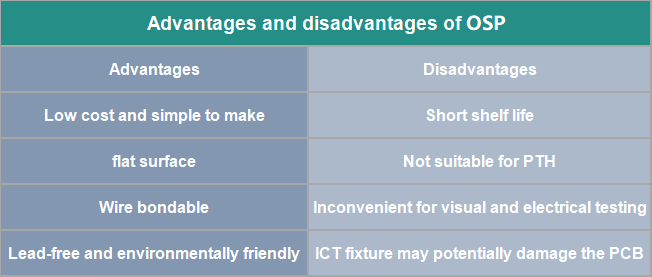
Advantages and disadvantages of OSP
- Immersion silver (ImAg)
ImAg, or Immersion Silver, is a process where a layer of silver is deposited on the clean bare copper surface through a chemical oxidation-reduction reaction.This silver layer provides oxidation resistance, heat shock resistance, and moisture resistance, ensuring solderability for Surface Mount Technology (SMT).
ImAg is an ideal choice for circuit boards with Electromagnetic Interference (EMI) shielding and is also used in membrane switches and aluminum wire bonding. The average surface thickness of silver is typically 5-18 microinches.
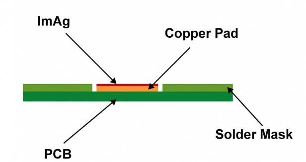
ImAg is more environmentally friendly compared to HASL and ENIG, and it has a lower cost compared to EMIG. Common applications include membrane switches, EMI shielding, and aluminum wire bonding.
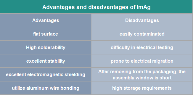
Advantages and disadvantages of ImAg
6.Electroless nickel electroless palladium immersion gold (ENEPIG)
ENEPIG coating consists of a layered structure of copper-nickel-palladium-gold, allowing for direct wire bonding to the coating.Compared to ENIG, ENEPIG has an additional palladium layer between nickel and gold, providing further protection to the nickel layer against corrosion and preventing the occurrence of black pads in ENIG surface finish.
The deposition thickness of nickel is approximately 3-6 μm, palladium thickness is about 0.1-0.5 μm, and gold thickness ranges from 0.02-0.1 μm in ENEPIG.
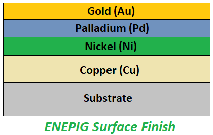
Common applications of ENEPIG include multi-layer PCBs, high-density components, and hybrid packaging technologies. It is frequently used in industries such as military, medical, and high-performance equipment.
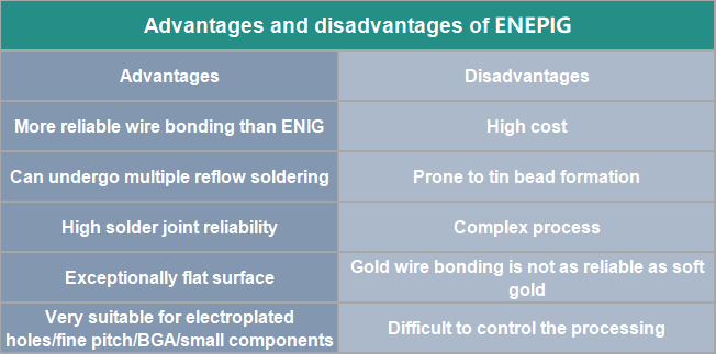
Advantages and disadvantages of ENEPIG
- Electrolytic Nickel/Gold
Electroplated nickel-gold is divided into "hard gold" and "soft gold."
Hard gold has a lower purity (99.6%) and is commonly used for gold fingers (edge connectors on PCBs), PCB contacts, or other areas prone to hard wear. The thickness of the gold layer can vary according to requirements.
Soft gold is purer (99.9%) and is typically used for wire bonding applications.
1)Electrolytic hard gold/gold finger plating
Electrolytic hard gold is a process where a layer of nickel followed by a layer of hard gold is deposited on the clean bare copper surface through electroplating. This hard gold layer exhibits resistance to alkaline etching, high hardness, and excellent friction resistance.
Hard gold is not suitable for wire bonding but is ideal for components that undergo frequent use and are prone to wear, such as PCBs, gold fingers, and case pads.
· Nickel thickness: 5-15μm
· Hard gold thickness: 0.75μm min or 1.27μm min
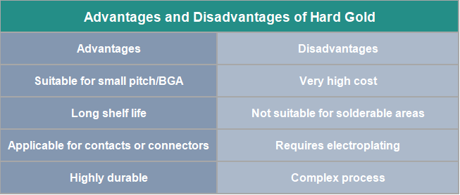
Advantages and disadvantages of Hard Gold
2)Electrolytic gold plating
Electrolytic gold refers to the process of depositing a layer of nickel followed by a layer of gold on a clean bare copper surface through electroplating. This nickel-gold layer provides alkaline etch resistance and ensures solderability for Surface Mount Technology (SMT), meeting the requirements of the bonding process.
· Nickel thickness: 3-8μm
· Soft gold thickness: 0.1-0.5μm
· Hard gold thickness: 0.5-1.5μm
Generally, under identical conditions with all other factors being equal, electroless nickel/gold is the most expensive PCB surface finish. However, certain applications indeed require the smoothness offered by electroless nickel/gold surfaces.
- Hybrid PCB Surface Finishes technology
Common combination methods:
· ENIG + HASL
· ENIG + Anti-Oxidation
· ENEPIG + ENIG
· ENEPIG)+ HASL
Above is the comparison of 7 PCB surface finish processes. If you want to reduce the manufacturing cost of PCB while meeting your requirements, you can compare the prices of various surface finish processes on AiPCBA. It can help you choose a satisfactory PCB surface finish process.
4.Choosing the right surface finish for a board
Surface finish is one of the most critical processes in PCB manufacturing, as it directly impacts process yield, rework quantities, testing capabilities, scrap rates, and costs. To ensure the high quality and performance of the final product, the following factors must be considered when selecting the appropriate surface finish process.
- Pad Flatness
The flatness of solder pads can impact performance and reliability. When making a choice, opt for a thin and uniform surface finish process, such as ENIG, ENEPIG, and OSP.
- Reliability and Wetting Properties
OSP and ENEPIG have low reliability; you may choose HASL.
- Wire Bonding
If PCB requires gold or aluminum wire bonding, choose ENIG and ENEPIG.
- Storage conditions
Some surface finishs have stringent requirements for storage conditions, such as OSP, while other processes enhance the durability of PCBs.
- Reliability
Consider the reliability requirements of the PCB throughout its entire lifespan and choose a surface finish that meets these needs.
- Cost
Different surface finish methods come with different costs. Choose a cost-effective finish based on the budget and project requirements.
- Soldering cycle
How long does it take for PCB soldering and rework? The details have been listed above; for instance, processes like Hot Air Solder Leveling (HASL) are not suitable for rework.
- RoHS Compliance
Typically, all surface finishs involving lead are not suitable for RoHS compliance and should be avoided.According to the specific requirements and characteristics of the PCB product, you can choose the appropriate surface finish process as indicated in the diagram below.

Printed Circuit Board Surface Finishes: advantages and disadvantages
5.Summarize
The above is an introduction to AiPCBA's PCB surface finish, covering 7 types of PCB surface finish, a comparison of PCB surface finish processes, and a summary of the advantages and disadvantages of PCB surface finish. We hope this information can help customers choose the appropriate surface finish process.
AiPCBA is the largest PCB/PCBA manufacturer in China, providing complex processes in the PCB manufacturing process with fast turnaround times and 24-hour delivery. If you have any PCB manufacturing needs, please feel free to visit AiPCBA.