Posted: May 14, 2022 by: Bonnie
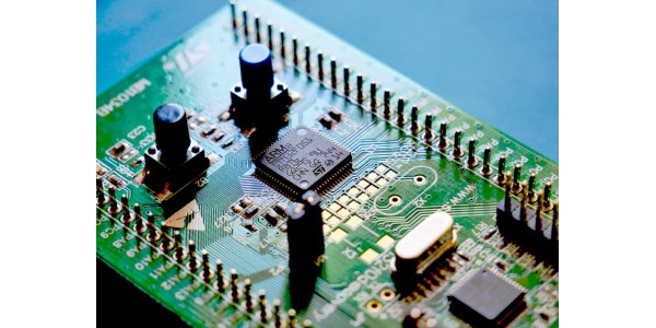
Printed circuit board ( PCB ) is an important electronic part, support for electronic components, and a carrier for the electrical connection of electronic components. Because it is made using electronic printing, it is called a "printed" circuit board. According to the complexity of electronic products, PCBs can be divided into single-sided PCBs to multi-layer PCBs. It can be classified as a simple through-hole or a blind & buried hole.
Printed circuit boards have developed from single-layer to double-sided, multi-layer, and flexible, and still maintain their respective development trends. Due to the continuous development in the direction of high precision, high density, and high reliability, continuous reduction in size, cost reduction, and performance improvement, printed circuit boards still maintain a strong vitality in the future development of electronic equipment.
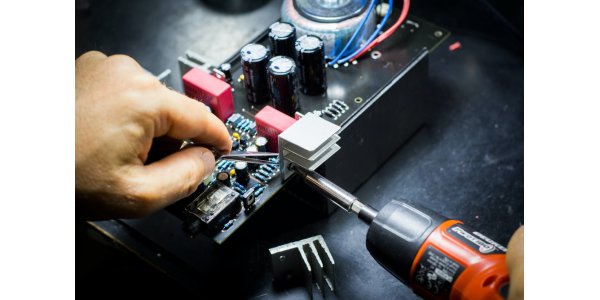
SMT (Surface Mounted Technology) mainly uses the placement machine to mount some small components on the PCB board. With the development of technology, SMT can also mount some large-sized parts, for example, some larger-sized mechanical parts can be mounted on the motherboard.
DIP(Dual In-line Package) is to insert parts on the PCB board. Because the size of the parts is large and it is not suitable for mounting or the manufacturer's production process cannot use SMT technology, the parts are assembled in the form of plug-ins. At present, there are two implementation methods of artificial plug-in and robot plug-in in the industry.
Turnkey PCB Assembly : AiPCBA is a turnkey PCB Assembly manufacturer. Turnkey PCB assembly service (one-stop PCB assembly) can offer one-stop service from PCB manufacturing, BOM sourcing, PCB assembly, SMT, THT, PCBA testing, product assembly, packaging, and delivery. AiPCBA has accepted many orders for turnkey PCB assembly from all over the world. To this day, it is still well received.
PCB Process Flow
Laminate Cut: It is the process of cutting the Raw Material into boards that can be made on the production line.
Inner Dry Film: It is the process of transferring the inner layer circuit pattern to the printed circuit board, including inner layer filming, exposure and development, inner layer etching, and other processes
Inner Etching: After the unexposed dry film/wet film is removed by the developer, the copper surface will be exposed, and the exposed copper surface will be dissolved and corroded with acid copper chloride to obtain the required circuit.
Brown Oxidation: A uniform organic metal layer structure with good adhesion characteristics is produced by chemical treatment so that the surface of the copper layer is controlled and roughened before the bonding of the inner layer, which is used to enhance the bonding strength between the copper layer of the inner layer and the prepreg after lamination.
Laminating: It is the process of bonding each layer of copper into a whole using the adhesion of pp. This bonding is achieved through the interdiffusion and penetration of macromolecules on the interface, and then interweaving.
Drilling: It makes through holes between the layers of the circuit board to achieve the purpose of connecting the layers.
Plate Through Hole: It is also called chemical copper. After drilling, the PCB undergoes a redox reaction in the chemical copper cylinder to form a copper layer to metalize the hole, so that copper is deposited on the surface of the original insulating substrate to achieve electrical communication between the layers.
Outer Dry Film: The same process as the inner layer of dry film.
Pattern Plating: The hole and circuit copper layer is plated to a certain thickness (20-25um) to meet the copper thickness requirements of the final PCB board. And etch away the unused copper on the board to expose useful circuit patterns.
Outer etching: The similar process as the inner layer dry film.
Solder Mask: It is one of the most critical processes in the production of printed circuit boards. It is mainly through screen printing or coating of solder mask ink, coating a layer of solder mask on the board surface, and exposure and development to expose the plates and holes to be soldered. Cover other places with a solder mask to prevent short circuits during soldering.
Silkscreen: The required text, trademark, or part symbol is printed on the board by screen printing, and then exposed on the board to ultraviolet radiation.
Surface Treatment: The solderability of bare copper itself is very good, but it is easy to be oxidized by moisture when exposed to the air for a long time. The most basic purpose of surface treatment is to ensure good solderability or electrical properties.
Routing: It refers to the outline treatment of the produced board according to the data in the Gerber data.
Testing: Using a flying probe test or a test fixture to check the electrical performance to detect whether there is open or short circuit.
PCB Assembly Process Flow
Programming and setting up the placement machine: According to the BOM pick & place file provided by the customer, program the coordinates of the position of the surface mount components.
Printing Solder Paste: The solder paste is stenciled to the pads of the PCB surface to prepare for the soldering of the components.
SPI (Solder paste inspection): The solder paste detector can detect the situation of solder paste printing and control the effect of solder paste printing.
SMT: Accurately install the electronic components of SMD on the fixed position of the PCB.
Reflow Soldering: The mounted PCB is reflowed, and the solder paste is heated to become liquid through the high temperature inside, and finally cooled and solidified to complete the soldering.
AOI: It is an automatic optical inspection, which can detect the soldering effect of the PCB board by scanning, and can detect the defect of the board.
Rework: Repair the defects detected by AOI or manually.
Plug-in: The components are processed with pins and inserted into the PCB board.
Wave Soldering: Perform wave soldering on the printed circuit board with the components inserted. During this process, liquid tin will be sprayed onto the PCB, and finally, the soldering is completed after cooling.
Cutting Feet: If the components pins of the soldered printed circuit board are too long, they need to be cut.
Post Welding Treatment: Hand soldering components with a soldering iron.
Cleaning the board: After wave soldering, the board will be dirty, it needs to be cleaned with board washing water and board washing tank, or cleaned with a machine.
QC: Check the PCB board, unqualified products need to be repaired, and qualified products can enter the next process.
PCBA Testing: PCBA testing can be divided into ICT test, FCT test, aging test, vibration test, etc.
AiPCBA’s advantage of PCB manufacturing and Assembly
AiPCBA's one-stop PCBA service, save you worry and energy: The most basic advantage is high efficiency and low cost. You don't need to purchase materials by yourself, you don't need to manage PCBA production projects by yourself, and you don't need to connect with multiple suppliers. You only need to safely hand over the production data to AiPCBA, and you can get your PCBA circuit board in about a week.
Efficiency advantages of resource centralization: AiPCBA focuses on improving the parts sourcing, PCB manufacturing, and PCBA processing capabilities of PCBA manufacturing, and improving the efficiency of all aspects of production. Various components and materials of PCBA products are collected and delivered in one factory, which can reduce the confirmation link of multiple inventory materials for back-and-forth delivery and receipt of component materials, which can save more than 3 days. Most of the passive components of your product can be directly called from the AiPCBA factory warehouse, and these materials can be flexibly deployed directly on the SMT production line, without considering the minimum packaging problem of material procurement, saving procurement time.
The Cost advantage of one-stop service: Your PCBA project will be produced by AiPCBA. AiPCBA's resources in all aspects are very concentrated, which will save you a lot of time in all aspects of PCBA production, shorten product delivery, help you avoid various material supply chain risks and manufacturing ability risks in advance, and can help you advance your product launch process and catch the business opportunities.
How to get the Quote service in AiPCBA
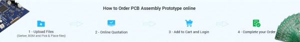
PCB quote: In our online PCB quotation system, you only need to upload the Gerber file and fill in the PCB specifications, you can easily get a quotation within 10 seconds. At the same time, our quotation page is also equipped with the function of an online Gerber 3D Preview. you can upload a Gerber file and have a 360-degree view of your PCB design.
BOM quote: AiPCBA's self-developed BOM quotation system can identify component information within 30 seconds, and analyze and quote market prices. And our BOM quotation system does not have strict requirements on the BOM format, all of which are based on the development of our strong R&D team, and play an extremely important role in our thousands of BOM price confirmations.
PCB Assembly Quote: Based on AiPCBA's PCB and BOM online quote system, we have also developed the calculation formula for assembly costs accordingly and combined these three quotation systems to form our complete one-stop PCBA quotation. As long as you upload the Gerber file and BOM list, our system will give you a complete PCBA quotation within 30 seconds.
AiPCBA also accepts Requests for a quotation by email, we are glad to receive your attachments (Gerber files, BOM list, etc. ) Pls feel free to contact us at sales@aipcba.com.
Why AiPCBA
AiPCBA has passed the national high-tech enterprise and ISO9001 quality system certification, has an intelligent storage system of more than 200,000 kinds of general electronic components, an advanced industrial IOT production line of 10,000 square meters, and a sound supply chain management and quality control system, helping 2 million small and medium-sized company around the world. Enterprises accelerate the process of product launch. We can sign the Mutual Confidentiality Agreement before the cooperation.
And we focus on one-stop PCBA intelligent manufacturing services, using artificial intelligence and big data technology, independently developed China's first PCBA flexible intelligent manufacturing platform AiPCBA®, integrating electronic components supply, product prototype, trial production, volume production, to provide customers with high-quality, high-efficiency quality services.
AiPCBA has always advocated, simplifying the customers’ work. Our customers only need to focus on design, and AiPCBA is responsible for purchasing and producing and delivering products at the fastest speed.