Posted: May 14, 2022 by: Bonnie
Printed circuit board(PCB) is an important electronic part, support for electronic components, and a carrier for the electrical connection of electronic components. Because it is made using electronic printing, it is called a "printed" circuit board. According to the complexity of electronic products, PCBs can be divided into single-sided PCBs to multi-layer PCBs. It can be classified as a simple through-hole or a blind & buried hole.
Types of Printed Circuit Boards
The diversification of PCB materials, layers, and processes are to suit different electronic products and their special needs. Therefore, there are many types of them. The following is a summary of some common distinction methods to briefly introduce the classification of PCB.
Organic Materials: Phenolic resin, fiberglass/epoxy resin, Polyimide, BT, etc.
Classifying PCB by flex or rigid
Rigid PCB, Flexible PCB, and Rigid-Flex PCB.
Single side PCB, double sides PCB, and multi-layer PCB
PCB Manufacturing Process Flow
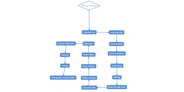
Laminate Cut
According to the requirements of the MI engineering data, the large sheets that meet the requirements are cut into small pieces for production, so as to meet the requirements of customers’ design.
Inner Dry Film
It is the process of transferring the inner layer circuit pattern to the printed circuit board, including inner layer filming, exposure and development, inner layer etching, and other processes.
Inner Etching
After the unexposed dry film/wet film is removed by the developer, the copper surface will be exposed, and the exposed copper surface will be dissolved and corroded with acid copper chloride to obtain the required circuit.
Brown Oxidation
A uniform organic metal layer structure with good adhesion characteristics is produced by chemical treatment so that the surface of the copper layer is controlled and roughened before the bonding of the inner layer, which is used to enhance the bonding strength between the copper layer of the inner layer and the prepreg after lamination.
Laminating
It is the process of bonding each layer of copper into a whole using the adhesion of pp. This bonding is achieved through the interdiffusion and penetration of macromolecules on the interface, and then interweaving.
Drilling
It makes through holes between the layers of the circuit board to achieve the purpose of connecting the layers.
Plate Through Hole
It is also called chemical copper. After drilling, the PCB undergoes a redox reaction in the chemical copper cylinder to form a copper layer to metalize the hole, so that copper is deposited on the surface of the original insulating substrate to achieve electrical communication between the layers.
Outer Dry Film
The same process as the inner layer of dry film
Pattern Plating
The hole and circuit copper layer is plated to a certain thickness (20-25um) to meet the copper thickness requirements of the final PCB board. And etch away the unused copper on the board to expose useful circuit patterns.
Outer etching
The similar process as the inner layer dry film.
Solder Mask
It is one of the most critical processes in the production of printed circuit boards. It is mainly through screen printing or coating of solder mask ink, coating a layer of solder mask on the board surface, and exposure and development to expose the plates and holes to be soldered. Cover other places with a solder mask to prevent short circuits during soldering.
Silkscreen
The required text, trademark, or part symbol is printed on the board by screen printing, and then exposed on the board to ultraviolet radiation.
Surface Treatment
The solderability of bare copper itself is very good, but it is easy to be oxidized by moisture when exposed to the air for a long time. The most basic purpose of surface treatment is to ensure good solderability or electrical properties.
Routing
It refers to the outline treatment of the produced board according to the data in the Gerber data.
Testing
Using a flying probe test or a test fixture to check the electrical performance to detect whether there is open or short circuit.
Final Quality Control (FQC)
Check the appearance, size, hole diameter, plate thickness, and marking of the board to meet customer requirements.
Items
Manufacturing Capabilities
Details
Number of Layers
1-20 Layers
Above 10 layers, please contact us.
Material
FR-4
For Aluminum, Flex, Rigid-flex, HDI, please contact us.
Max. PCB Size (Dimension)
500×550mm
Beyond this dimension, please contact us.
Dimension Tolerance (Outline)
±0.2mm/±0.5mm
±0.2mm for CNC routing, and ±0.5mm for V-scoring.
Board Thickness
0.2-2.4mm
Above 2.0mm or below 0.6mm, please contact us.
Thickness Tolerance (T≥1.0mm)
±10%
Ranges from (T-T×10%) to (T+T×10%)
Thickness Tolerance (T<1.0mm)
±0.1mm
Ranges from (T-0.1) to (T+0.1)
Min. Trace/Spacing
3.5mil
Suggest to design trace/spacing above 5mil to save cost.
Outer Layer Copper Thickness
1oz/2oz (35um/75um)
Greater than 2oz, please contact us.
Inner Layer Copper Thickness
0.5oz/1oz (17μm/35μm)
Greater than 1oz, please contact us.
Drill Hole Size (CNC)
0.2-6.3mm
The finished hole diameter will be smaller than size of drill bits because of copper plating in the hole.
Hole Size Tolerance (CNC)
±0.08mm
For example, drill size is 0.6mm, the finished hole size ranges from 0.52mm to 0.68mm.
Min. Via Hole Size
0.2mm
For multilayer PCB only.
Min. Via Diameter
0.45mm
For multilayer PCB only.
Via to Trace
≥5mil
Minimum distance between via (plated hole) and trace is 5mil.
Trace to Outline
≥0.2mm
For individual board (routing) only. If ship as panel with v-scoring, trace to v-cut line is no less than 0.4mm.
Min. Width of Annular Ring
0.15mm (6mil)
For Via in Pad only.
Annular Ring
≥3mil
For annular ring surrounded by traces.
Min. Character Width (Legend)
0.15mm (6mil)
Less than 0.15mm width will be too narrow to be identifiable.
Min. Character Height (Legend)
0.8mm (32mil)
Less than 0.8mm height will be too small to be recognizable.
Character Width to Height Ratio (Legend)
1:5
Most suitable ratio in silkscreen legends processing.
Min. Edge Rails
3mm
Lear more PCB Manufacturing Capabilities
As you know, the manufacturing process of printed circuit boards is long and difficult. To ensure that your PCBs are of the quality, performance and durability you expect, you must choose a manufacturer with a high level of expertise and a strong focus on quality in every manufacturing process.
AiPCBA specializes in the following businesses: flexible PCB, custom PCB, prototype PCB, turnkey PCB assembly, quick turn PCB assembly, electronic PCB assembly, small batch PCB assembly, etc.
All PCBs in AiPCBA are produced based on UL and ISO certification standards. All our normal specification PCBs are strictly obeying to IPC-A-6011/6012 Class 2 latest version and IPC-A-600 Class 2 latest version.
AiPCBA online intelligent manufacturing service provides quick PCB prototype and volume production services for 1 million small and medium-sized customers around the world. The entire process of customer online ordering, evaluation, production process monitoring, and delivery is completed online in the cloud.
Starting to contact with AiPCBA now!