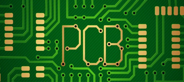
Introduction
Electronic components are developing towards continuous optimization. In the design of PCB, it is necessary to summarize High-frequency routing skills according to relevant hardware design experience, and thus reduce the signal interference during the design process. On the other hand, designer can better improve the performance of High-frequency PCB through reasonable placement and layout of electronic components in other parts.
High-frequency PCB layout
First, the designer must have enough knowledge of the characteristics of the electronic components that need to be used. Then, through the mechanical structure of PCB, product quality and other factors, the reasonable planning and partition design of PCB is completed. It will not only extend the service life of the PCB, but also improve the performance and stability of PCB.
1. The mechanical structure factors
1)Designers should confirm the appearance shape, size, thickness and material requirements of PCB,and they should confirm the PCB is rigid printed board or flexible printed board at the same time.
2) Designers should to confirm the accuracy of the positions of the relevant structural parts of the printed board (For example:locking bars, cold plates, plate clamps, mounting screws, studs, and so on). On the other hand, they also need to consider the location and size of the mounting holes in the printed board, as well as whether the PCB is hold on pad or whether the PCB is metallized.
3) Designers should pay attention to the location of connectors, indicator lights, power sockets, switches and other electronic components.
4) Designers should place the Light-emitting diode exactly where they are. The power socket and connector also should be designed at the edge of the PCB, and it should be kept at a reasonable distance.
5) Designers should put some switches and fine-tuning components on the edges of the PCB. Because they can get more convenience when they make overall alignments and connections.
For components that need to be replaced frequently during use, they must be placed in areas with fewer electronic components to facilitate operation and replacement during use. For devices with high relative mass, supports should be used to fix the devices during the design process, while for some larger and heavier components, and reasonable planning should be carried out instead of directly placing them on the PCB surface.
In the High-frequency working state, usually power supply, transformer, High-power tube, rectifier tube, CPU, storage and other devices will emit a large amount of heat, so in the layout design. It is necessary to give full consideration about the heat dissipation and ventilation of these components. Here are some questions to pay attention to:
1)The heating devices as far as possible to disperse distribution, so that the veneer surface heat consumption uniform. Do not placing thermosensitive devices or devices with High-power consumption close to each other, such as crystal oscillator, memory, CPU, etc.
2)Designer should Make thermally sensitive components arranged in the coldest region. About the natural convection of the shell sealing cooling equipment, they should put thermally sensitive devices at the bottom and the components of high heat as upper. If the enclosure is not sealed, designer should place the thermosensitive device at the cold air inlet. For the forced convection cooling equipment, they can place in the heat sensitive components at the air inlet.
3) When the designer needs to arrange a series of devices along the direction of air flow and incoming flow to dissipate heat, the electronic components should be staggered along the direction of airflow as far as possible to reduce the interaction between upstream and downstream devices. But if they cannot be misaligned, designers should avoid placing bigger electronic components (or structural components) on the intake side.
3. The layout of several general types of devices
1) The power supply device factors
A. The primary power supply device is generally placed in the nearest area of the main power inlet of the backplane connector.
B. The secondary power supply can be placed near the device that needs the power supply according to the use condition, and the smooth flow of the power supply should be considered at the same time.
C. The independent switching power supply module should not be placed within 1 inch of the edge of the single board and should be 2 inches away from the external interface.
2) The timing device factors
A. The timing device used for a single component should be as close as possible to the component.
B. The timing device used for multiple components are placed in the center of each component to ensure that the signal length to each node is not too long.
C. The timing circuit should be away from the edge of the board and away from the interface connector layout at the same time.
3) PLL filter element, analog signal filter element factors
The filter circuit shall be placed strictly in accordance with the topology specified in the device manual. The filter capacitance should be as close to the filter signal pin as possible. Under the filter and beside the device, there should be no strong periodic signal such as clock running.
4)Capacitance factors
A. The filter capacitance of the power chip should be placed according to the recommended layout given by the power chip.
B. The High-frequency filter capacitance of BGA (Ball Grid Array Package) chip should be placed on the back of BGA close to the pin as far as possible.
C. The energy storage capacitor should be placed between the output of the power chip and the device (preferably evenly placed).
D. The High-frequency filter capacitance of a non-BGA encapsulated chip should be placed as close as possible to the front of the chip and the pin, or as close as possible to the back of the chip and through the hole.
E. The placement method of the energy storage capacitor refers to the BGA chip.
F. The coupling capacitance sent by PCIE should be placed close to the sending end.
G. High-speed AC coupling capacitance should be close to the receiving end except PCIE.
5)Resistance factors
A. In principle, there is no special requirement for the placement of pull-up resistors. However, there is an exception: As a multiplexed pin(For example, data, addresses, or pins of control for a processor's local Bus, Ethernet, or other buses), it is necessary to consider the minimum length of the routing branch caused by the port on resistance in order to avoid affecting the reliability of the bus communication.
B. Series matching resistors should be placed as close as possible to the origin port.
C. Parallel matching resistors are placed as close to the terminal as possible.
D. The filter resistance should be placed as close as possible to the pin of the filter.
6)Digital hybrid circuit factors
A.The device layout should take account of the different partitions of the digital-analog circuit for different placement.
B. Between the analog and digital power sources, the coppers on the ground plane cannot be coupled to each other. The routing of the respective power supply and signal trace should refer to the respective ground plane to avoid crosstalk.
C. Integrated circuits that have both analog and digital components need to be placed across partitions.
D. The Digital-to-Analog conversion circuit shall be arranged at the junction of the digital and analog regions.
4. The electromagnetic interference
Designers should minimize electromagnetic interference during the design process.
In general, designers can choose to shield or reduce the speed of High-frequency electronic devices, reducing the circuit or increasing the dielectric constant of PCB to eliminate electromagnetic interference. On the other hand, the decoupling capacity of the integrated circuit, they need to choose closer distances to be placed so that they can minimize the amount of interference caused by the battery. At the same time, as the High-voltage components, designers need to try to design people's hands that are not easy to touch when people are debugging. This will ensure the safety of the components in the process. Finally, about those elements that interact with each other, the designers will be effectively partitioned. It will make the electronic components not too close to each other when they can interfere with each other. Between input and output of different components, which should reduce feedback interference.
In AiPCBA, we has established the most efficient and strongest rapid manufacturing platform in the field of PCB prototypes and multi-variety small and medium volume. Providing rapid prototype and volume production manufacturing services for advanced electronic products for many technologically innovative enterprises, including small and micro enterprises. Build a team of senior PCB technical consultants and experts, combined with the supporting multi-variety rapid PCB assembly capabilities, to provide customers with personalized one-stop outsourcing services.
High-frequency PCB routing
As High-frequency PCB has high integration in the running process and the density of the routing is large. In general, when the designers are designing the process, it is in order to reduce the impact of the associated interference, so that they try to choose the multi-layer board for the routing. The designer selects a reasonable layer of structure, and then they can fully use the surface layer of the ground to make good shielding to achieve the nearest ground. At the same time, this will also be able to minimize the return flow path between the signal and the power supply and the corresponding plane, so that the impact of the cross interference between the signals in the transmission process is reduced. The higher the number of layers of the PCB, the higher the cost level of the PCB is made. So, when the designers want to design the PCB, and they need to select the appropriate plate layer and design according to the reliability and specific situation of the relevant circuit. Designer only make a routing planning before starting, and they can make the PCB achieve good usability.1. The routing principle
1) Basic principle
A. The shorter the wires between different circuit elements, the higher the transmission efficiency and the less interference at the same time.
B. During the design process, the routing should be done in the form of straight lines and bending, and sharp angles should be avoided as far as possible. If it is necessary to turn transition the situation, the designer should adopt the circular arc design for effective transition.
C. For the routing in the High-frequency PCB, it is better to take different ways between adjacent layers. The routing can be done alternately horizontally or vertically to minimize interference.
D. The spacing between the lines and the center of the line should meet the principle of 3W (three times the line width) as far as possible to reduce crosstalk between signals.
2) High-speed serial signal routing
A. Routing of PCIE, SATA, Ethernet, differential network port and other signals shall meet the requirements of High-speed signal routing:
- With a complete reference plane,
- Sending and receiving signals in the same group require the same length of the same layer,
- The distance between the center of line and line satisfies the principle of PCB layout 3W principle,
- Prevent crosstalk caused by long distance parallel routing,
- PHY the chip is as close to the transformer as possible, and the routing is as short as possible.
B. Obvious impedance mutation factors should be avoided during the routing process.
For example: discontinuity of reference plane, crossing dense pore area, too close to plate edge or mounting hole, etc.
C. If High-speed signal has cross - sectional routing, it should be considered to use capacitance way for partition short, and it ensure the minimum path of backflow signal.
D. For High-speed signal lines, especially for differential line layer change, GND hole should be placed near the layer change hole for shielding.
E. For important High-speed signal lines, such as clock signal routing, ground design should be carried out on both sides of the routing line.
F. When High-speed signal routing is arranged in the inner layer and the routing length is greater than 1/20 of the wavelength corresponding to signal frequency, the inner microstrip line or cladding design should be adopted.
3) Internal parallel bus routing
A. Local Bus and PCI routing should be used in Daisy chain way.
B. The reference clock or running clock of the parallel bus should be wired to avoid other signals, and they should not overlap with adjacent signals for long distances.
C. If the gigabit Ethernet Interface is designed as RGMII, the sending and receiving signals should be wired equally.
4) Note for clock signal routing
A. The spacing between the same layer and other signals should be separated as far as possible, and they cannot be too close to each other.
B. The adjacent layers should avoid long distance overlapping trace with other signals.
C. When the crystal oscillator circuit is running, attention should be paid to the isolation design of crystal oscillator envelope.
5) Routing of special devices or signals
A. The input signal line and output signal lines of the filter (filter circuit) should not be parallel or crossed with each other.
B. The PCB below the inductor coil should not have High-speed routing or sensitive control routing. (If unavoidable circumstances are encountered, the designer must consider the direction of the coil. And they must keep the direction of the field intensity parallel to the plane of the coil to minimize the number of magnetic lines of force passing through the coil.)
C. The projection layer below the inductance of the power supply should be banned. At the same time, the inductance must not have the sensitive signal near the wire, so as not to interfere with the coupling.
E. Differential mode inductance is mainly used to suppress differential mode interference of power supply circuit. As for prevent interference coupling, other sensitive signals or devices should not be close to differential inductance.
F. Protective devices protect the line as thick, short and uniform as possible. The protection ground cannot be connected to any device or ground wire except for the protection device. A safe distance should be maintained between the protected ground and other bonding pads, routing and copper laying.
G. TVS should be placed near the interface with thin and thick routing. The gas discharge tube should be connected to the protective ground when protecting the ground, and the line width of the routing should meet the maximum flow capacity of discharging energy.
-The isolation transformer shall control the primary stage routing loop.
-The projection layer below the transformer is banning routing to prevent the interference coupling between front and rear stages.
-The running length of transformer and connector shall not be greater than 1 inch.
2.Power cord and ground wire
1) The power supply plane should not have large loops.
2) The width of the power supply plane shall meet the requirements of the over-current capacity of the power supply.
3) The reference between the inner power source plane and its ground plane needs to be shrunk (meeting the 20H principle).Different power supply planes of adjacent layers should be avoided overlapping, especially the power supply with greater interference should not overlap with sensitive power supply.
4) The perforation between the inner power supply and the ground plane adopts the cross-connection mode of flower welding plate, which is to prevent the heat loss too fast during welding and lead to virtual welding. If some power supply overflows, the through-hole can be changed into solid connection copper-laying mode according to the actual situation.
3.Integrated chip routing
In the design of integrated chip circuit, the hf decoupling capacitors should be reasonably designed and placed, and the positions of capacitors and IC circuits should be reasonably planned to achieve good operation results.
4.Apply the copper handle
As for enhance the Anti-interference ability between different circuits, the related circuits should be treated with copper coating. Copper coating is designed to help the PCB dissipate heat effectively and enhance the strength of the PCB. At the same time, it can also effectively shield the relevant grounding wires. Therefore, when applying copper, designers should try our best to choose the raster-like thinness, which is to ensure that copper application can achieve a good shielding effect.
In the process of High-frequency PCB design, according to the different features of the original copy of the reasonable planning and design, designer should fully consider the interference between electrical components of the design process, the reasonable partition to the position of the components, and selecting the appropriate methods and techniques to guarantee the accuracy of routing, thus improve the overall stability and rationality of High-frequency PCB.
Electronics industry is fast-paced and companies can’t simply survive without changing or upgrading products as per consumer demands and on-going innovation is the key to extra ordinary success, if product is not quickly marketed with reliable custom printed circuit board assembly partner one won’t be able to move one step ahead then competition. So it is important and crucial for Business to have quality custom printed board assembly service provider.
AiPCBA provide PCB manufacturing and assembly service. We have customers from different industries in terms of cost-effectiveness, quality, delivery and any other requirements. From PCB layout to PCB prototyping, mass manufacturing, and then PCB assembly, electronic box assembly services, our printed circuit boards are widely used in robotics, medical, automotive, communications, industrial and consumer electronics products.
AiPCBA® online intelligent manufacturing service provides quick PCB prototype and volume production services for 1 million small and medium-sized customers around the world. The entire process of customer online ordering, evaluation, production process monitoring, and delivery is completed online in the cloud.