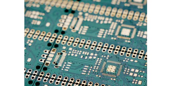
What is Solder Mask?
Solder mask is a thin layer of polymer used on PCB to prevent solder joints from bridging. The solder mask can also prevent oxidation and be applied to the copper trace on the PCB board. As a protective coating on the copper trace, PCB welding mask can prevent rust and prevent solder from forming a bridge leading to short circuit. There are 3 main types of PCB solder mask : Epoxy liquid, liquid imageable, dry film photo-imageable. There are four types of solder mask, and the decision on which one to use depends on a variety of factors - including the physical size of the PCB, the final application to be used, holes, components to be used, conductors, surface layout, etc.
AiPCBA has led the PCB industry for over 7 years, offering the industry's most advanced printed circuit board technology and the highest quality standards. You can customize your PCB at AiPCBA. From the simplest printed circuit boards to the most complex low-volume and large-scale production, AiPCBA has the capability to meet all your contract electronics manufacturing needs.
All PCBs in AiPCBA are produced based on UL and ISO certification standards. All our normal specification PCBs are strictly obeying to IPC-A-6011/6012 Class 2 latest version and IPC-A-600 Class 2 latest version.
Learn More about AiPCBA’s PCB manufacturing!
3 types of PCB solder mask
(1) Epoxy liquid solder maskEpoxy is the cheapest alternative to welding masks. Epoxy resin is a polymer screen printed on a PCB. Screen printing is a printing method that uses a fabric mesh to support ink blocking patterns. The grid allows recognition of open areas for ink transfer. In the last step of the process, thermal curing is used.
(2) Imaging liquid mask solder mask
The liquid light imaging mask, also known as LPI, is actually a mixture of two different liquids. Liquid components are mixed before application to ensure a longer shelf life. It is also one of the more economical products among four different PCB solder resist types. LPI can be used in screen printing, screen coating or spraying applications. Mask is a mixture of different solvents and polymers. As a result, a thin coating can be extracted and adhered to the surface of the target area. This mask is intended for soldering masks, but PCB does not require any final plating coating currently available.
In contrast to the old epoxy ink, LPI is sensitive to ultraviolet light. The panel needs to be covered with a mask. After a short "curing cycle", the circuit board is exposed to ultraviolet light using photolithography or ultraviolet laser. Before applying the mask, the panel needs to be cleaned and there is no sign of oxidation. This is done with the help of special chemical solutions. It can also be done by scrubbing the panel with an alumina solution or with suspended pumice.
A dry film photo-imageable welding mask is used, and a vacuum lamination is used. The dry film is then exposed and developed. After developing the film, the openings are positioned to produce patterns. After that, the component is soldered to a copper pad. The copper layer is then pressed onto the circuit board using electrochemical treatment. Copper is stratified in the hole and trace area. Tin is ultimately used to help protect copper circuits. In the final step, the film is removed and the etched marks are exposed. This method also uses thermal curing. Dry film solder mask is usually used for high density terminal blocks. As a result, it does not flood into the through hole. These are some of the positive factors for using dry film solder masks.
The production process of Solder mask
(1)Solder mask ink mixing: The main agent and hardener of the ink are pre-stirred by hand, and then the ink is completely mixed evenly by mechanical vibration. At the same time, leave it for about 15 minutes to eliminate air bubbles, and the mixed ink needs to be used within 24 hours.(2)Board pretreatment: Remove oxides, oil stains and impurities on the board surface, and roughen the copper surface to enhance the adhesion of ink to the board surface.
(3)Coating of ink: According to customer requirements, the ink is evenly coated on the board surface by screen printing or curtain coating.
(4)Treatment with low temperature: The solvent in the wet ink is evaporated, and the ink on the board is initially hardened to prepare for exposure.
(5)Exposure: According to customer requirements, a specific exposure negative film is made on the board and exposed under ultraviolet light. The ink with the shading area will eventually be washed away to expose the copper surface, and the part exposed to the ultraviolet light will harden and finally adhere to the board surface.
(6)Development: Wash off the ink with the shading area during exposure, and the board surface will fully meet the customer's requirements after development.
(7)UV curing: Increase the surface gloss, enhance the heat resistance and chemical properties of the solder mask on the board, and at the same time harden the ink on the board to avoid scratching the oil surface in subsequent operations such as character printing.
(8)Silkscreen printing: Symbols printed according to customer requirements.
(9)Treatment with low temperature: The ink is completely cured, and a stable cross-linked network structure is formed on the surface to meet the electrical and physical and chemical properties of the ink. The pencil hardness test should be above 6H as normal.
Turnkey PCB Assembly in AiPCBA
We have over 7 years of knowledge and combined experience in rendering high tech PCB assembly service, PCB manufacturing service and different PCB assembly technologies like Through-hole (THT) and Surface Mount (SMT). Mainly, we work with three types of printed circuit boards including Rigid PCB, Flexible PCB and metal core PCB.Whether your technology includes Surface Mount (SMT), Through-hole, or a mixed technology for single or double-sided boards in small quantities, prototypes, or large production runs, AiPCBA has the ability to provide for all of your contract electronics manufacturing needs.
Learn more about AiPCBA’s Turnkey PCB Assembly!
How to get the Quote in AiPCBA
PCB quote: In our online PCB quotation system, you only need to upload the Gerber file and fill in the PCB specifications, you can easily get a quotation within 10 seconds. At the same time, our quotation page is also equipped with the function of an online Gerber 3D Preview. you can upload a Gerber file and have a 360-degree view of your PCB design.
BOM quote: AiPCBA's self-developed BOM quotation system can identify component information within 30 seconds, and analyze and quote market prices. And our BOM quotation system does not have strict requirements on the BOM format, all of which are based on the development of our strong R&D team, and play an extremely important role in our thousands of BOM price confirmations.
PCB Assembly Quote: Based on AiPCBA's PCB and BOM online quote system, we have also developed the calculation formula for assembly costs accordingly and combined these three quotation systems to form our complete one-stop PCBA quotation. As long as you upload the Gerber file and BOM list, our system will give you a complete PCBA quotation within 30 seconds.
AiPCBA also accepts Requests for a quotation by email, we are glad to receive your attachments (Gerber files, BOM list, etc. ) Pls feel free to contact us at sales@aipcba.com.