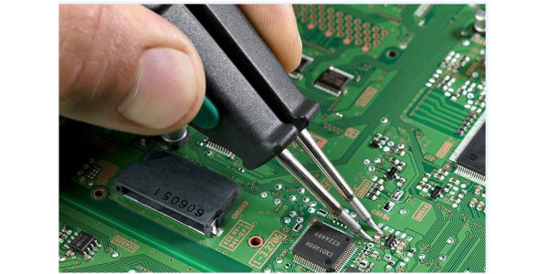
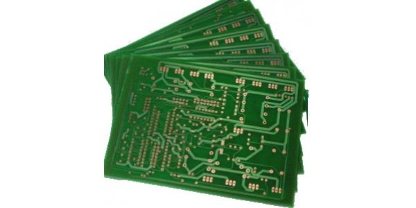
OSP is the abbreviation of Organic Solder-ability Preservatives. Simply put, OSP is to grow a layer of organic film on a clean bare copper surface by chemical methods. This layer of film has anti-oxidation, thermal shock, and moisture resistance to protect the copper surface from continuing in the normal environment. Rusting (oxidation or vulcanization, etc.); however, in the subsequent high-temperature soldering, this protective film must be easily removed by the flux, so that the exposed clean copper surface can be melted with the molten solder in a very short time Immediately combine to become a solid solder joint.

OSP manufacturing flow:
Degreasing-->Secondary Water Washing-->Micro Erosion-->Secondary Water Washing-->Acid Washing-->DI Water Washing-->Film-forming Air Drying-->DI Water Washing-->Drying
1) Degreasing
The quality of the oil removal effect directly affects the quality of the film formation. If the oil removal is not good, the film thickness is uneven. On the one hand, the concentration can be controlled within the process range by analyzing the solution. On the other hand, you should always check whether the degreasing effect is good. If the degreasing effect is not good, you should replace the degreasing fluid in time.
2) Micro-erosion
The purpose of micro-etching is to form a rough copper surface to facilitate film formation. The thickness of the micro-etch directly affects the film formation rate. Therefore, to form a stable film thickness, it is very important to maintain the stability of the micro-etch thickness. Generally, it is more appropriate to control the micro-etching thickness at 1.0-1.5um. Before each shift production, the micro-etching rate can be measured, and the micro-etching time can be determined according to the micro-etching rate.
3) Film formation
It is best to use DI water for the water washing before film formation to prevent the film formation liquid from being contaminated. It is also best to use DI water for the water washing after film formation, and the PH value should be controlled between 4.0-7.0 to prevent the membrane layer from being contaminated and destroyed. The key to the OSP process is to control the thickness of the anti-oxidation film. The film is too thin, and the thermal shock resistance is poor. During over-reflow soldering, the film layer is not resistant to high temperatures (190-200°C), which ultimately affects the welding performance. On the electronic assembly line, the film cannot be well dissolved by the flux , Affecting welding performance. Generally it is more appropriate to control the film thickness between 0.2-0.5um.

OSP PCB SMT application guide:
1) The organic coating on the OSP PCB surface is extremely thin. If exposed to high temperature and high humidity for a long time, the PCB surface will oxidize and the solder-ability will deteriorate. After the reflow soldering process, the organic coating on the PCB surface will also become thin, resulting in PCB copper foil is easily oxidized. Therefore, the OSP PCB material should be vacuum-packed with a desiccant and humidity display card. During transportation and storage, use separation paper between PCBs with OSP to prevent friction from damaging the OSP surface. And it should not be exposed to direct sunlight, keep a good warehouse storage environment, relative humidity: 30~70%, temperature: 15~30℃, storage period is less than 6 months. When unpacking at the SMT site, you must check the humidity display card and put it online within 12 hours. Never open a lot of packages at once, in case it can't be finished, or if there is something wrong with the equipment, it will take a long time to solve it. It is easy to go wrong.
2) The opening area of OSP is slightly larger than that of ordinary tin-sprayed steel mesh, so when the PCB is changed from tin-spray to OSP, the steel mesh should be re-opened to ensure that the solder can cover the entire pad. The principle of tinplate can be used for the engraving of steel plates. Considering that OSP is flat, it is beneficial to the formation of solder paste, and PAD can not provide a part of solder, so the opening can be increased appropriately. After the opening is enlarged, in order to solve the problem of SMT CHIP parts solder beads, tombstones and OSP PCB exposed copper, the solder paste printing machine steel mesh opening design method is changed to a concave design.
3) OSP PCB printing should try to avoid printing errors, because cleaning will damage the OSP protective layer. When the PCB printing solder paste is bad, because the OSP protective film is easily eroded by organic solvents, all OSP PCBs cannot be soaked or cleaned with highly volatile solvents. It is recommended to wipe the solder paste with a non-woven cloth and 75% alcohol. When re-work is completed, the SMT soldering operation on the PCB surface of the current rework should be completed within 2 hours.
4) The peak temperature should not be set too high (240-245°C) during reflow soldering, and the time in the furnace should be well controlled, otherwise the soldering problem of the pad may occur when the second side is made. Of course, this situation also explains The high temperature resistance of the board is not enough. For double-sided assembly, the first reflow requires a nitrogen environment to maintain the solder-ability of the second side. The current OSP will also disappear when there is flux and heat, but the protective agent on the second side remains intact until solder paste is printed or over-wave soldering, and inert gas environment is not necessarily required during reflow or wave soldering.
5) OSP surface treatment should be used for ICT testing of OSP PCB. If the test point is not covered by solder, it will cause contact problems of needle bed fixtures during ICT testing. There are many mission factors that will affect the ICT test results. Some of these factors are: the type of OSP provider, the number of passes in the reflow furnace, whether it is a peak process, nitrogen reflow or air reflow, and the type of simulation test during ICT. Simply changing to a sharper probe type through the OSP layer will only cause damage and puncture the PCA test vias or test pads. Therefore, it is strongly recommended not to directly detect the exposed copper pads. It is required to consider adding tin to all test points when opening the steel mesh.
