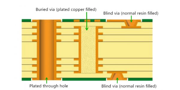
Blind holes are located on the top and bottom surfaces of the printed circuit board and have a certain depth. They are used for the connection of the surface layer circuit and the inner layer circuit below. The depth of the hole usually does not exceed a certain ratio (aperture). AiPCBA has the ability to manufacture blind and buried via PCB. Despite the higher cost of this technology, we have experience in purchasing quality factories to reduce prices. The use of blind holes and buried holes in the design of multi-layer PCBs will increase the cost and increase the difficulty of manufacturing than through-holes. Laser drilling or multiple presses are required, and it is easier to produce more scrap.
Since blind vias must be drilled through only some layers, they must be drilled and plated before the board layers are completely combined. Thus, multiple lamination steps are required compared to one lamination for through holes. These extra steps add time and cost to your order. However, the benefits of this technology outweigh the extra cost in many cases.

With the miniaturization of electronic products, the designers of components and printed circuit boards need to work in the shrinking space to maintain competitiveness, which makes it necessary to use blind holes to form interconnection between layers in many cases. Depending on the size of the package, sometimes only one blind hole drilling cycle may be used to meet the requirements. However, in many cases, multiple groups of blind holes must be formed and stacked on top of another group until the device is fully connected. To this end, manufacturers use multiple drilling and laminating cycles in a process known as high density interconnect (HDI).
HDI is optional and is usually required. However, it does increase manufacturing costs significantly, so it is necessary to understand the impact of adding blind holes in the design. There are several ways to add blind holes (and / or buried holes) to a PCB. When the material is still in its core form (before any lamination) or the layers of some layers can be pressed together, some underground structures before blind hole mechanical drilling can also be carried out. The through-hole is first drilled from the top of the core or substructure to the bottom, then conventional plating is carried out, and then it enters another lamination stage. The interconnection quality using this method is very good because the plating solution can flow freely through temporary openings. You can then fill the holes before laminating the substructure to the remaining layers.
As a result of multiple lamination stages (at least one more layer than normal) plus drilling, plating, filling and casting, the cost of this method began to increase the need for image processing for each subgraph. If the outer pad needs to be restored to its original good condition for surface mount assembly installation (via in PAD), such treatment will increase the cost.
