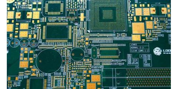
As the basic unit of PCB surface mount assembly, pad is used to form the pattern of PCB pad. Rich pad knowledge is essential for an excellent PCB engineer.If the two ends of SMD components are not connected with plug-in components, test points with diameter equal to or greater than 1.8 mm should be added to facilitate on-line tester testing. If the IC pin pad with dense pin spacing is not connected to the manual plug-in pad, a test pad should be added. If it is a chip IC, the test point cannot be placed in the chip IC silk screen.
The diameter of the test point is equal to or greater than 1.8 mm, which is convenient for on-line tester.If the pad spacing is less than 0.4 mm, white oil shall be laid to reduce the continuous welding during wave crest. Both ends and ends of SMD components shall be designed with tin lead. The width of tin lead is recommended to be 0.5 mm, and the length is generally 2 or 3 mm. If the single panel has hand soldering components, the tin bath should be removed in the opposite direction to the tin passing direction. The width of the hole is 0.3 mm to 1.0 mm (50-70% of the aperture).

The spacing and size of conductive rubber keys should be consistent with the actual size of conductive rubber keys. The PCB board connected with this should be designed as gold finger, and the corresponding gold plating thickness should be specified. The size and spacing of pad should be the same as that of SMD (1:1). For the solder joints whose distance between pads (more than 4 pads) on the same line is less than 0.4 mm, on the basis of adding white oil, if the long side of the component is parallel to the wave crest direction as far as possible, an empty pad is added at the end of the pad or the pad at the end is enlarged to eat the trailing solder and reduce the continuous welding.
In conclusion:
1) If the two ends of SMD components are not connected with plug-in components, test points with diameter equal to or greater than 1.8 mm should be added to facilitate on-line tester testing.
2) If the IC pin pad with dense pin spacing is not connected to the manual plug-in pad, a test pad should be added. If it is a chip IC, the test point cannot be placed in the chip IC silk screen. The diameter of the test point is equal to or greater than 1.8 mm, which is convenient for on-line tester.
3) If the pad spacing is less than 0.4 mm, white oil shall be laid to reduce the continuous welding during wave crest.

4) Both ends and ends of SMD components shall be designed with tin lead. The width of tin lead is recommended to be 0.5 mm, and the length is generally 2-3mm.
5) If the single panel has manual welding components, the tin bath should be removed in the opposite direction to the tin passing direction. The width of the inspection hole is 0.3 mm to 1.0 mm.
6) The spacing and size of conductive rubber keys should be consistent with the actual size of conductive rubber keys. The PCB board connected with this should be designed as gold finger, and the corresponding gold plating thickness should be specified.
7) The size and spacing of pad should be exactly the same as that of SMD.
