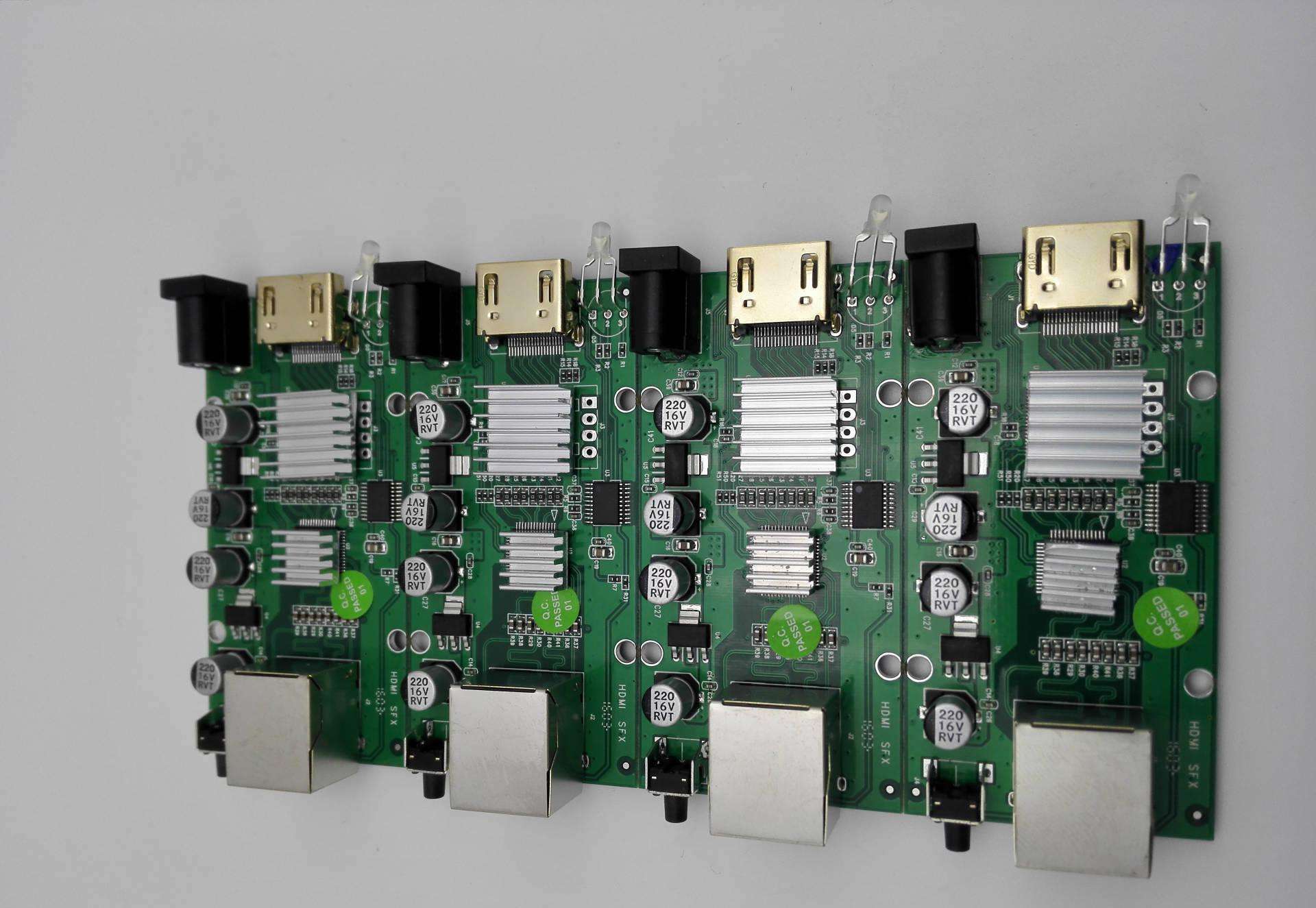
Speak of SMD, Surface mounted devices is one of SMT (surface mount technology) components. In the initial stage of electronic circuit board production, the through hole assembly is completely completed by human. After the introduction of the first batch of automation machines, they can place some simple pin elements, but complex elements still need to be placed manually before reflow welding. Surface mounted components mainly include rectangular, cylindrical, composite and special-shaped components.
Before SMD soldering, you need to prepare some consumables, such as: solder wire (leaded), solder paste (leaded), flux, soldering iron, flux pen, T12 soldering station, reflow oven, IPA (isopropyl alcohol) Suitable for cleaning (for local use), etc. The specific case should be adjusted according to the welding requirements. There are five basic steps that involved in the process of soldering SMD to a PCB pad.
Step 1: Check and clean the PCB
For precision parts, the fine particles remaining on the surface of the product exceeding the specified limits will directly affect the tightness of the product during assembly and accelerate the wear and aging of the product; for electronic assembly circuit boards, excessive residual ion content on the surface will cause The electrical safety of the product in long-term use may cause electrochemical leakage due to ion migration, resulting in product damage.
Step 2: Paste the solder paste onto the PCB
Make a steel mesh, the holes on the steel mesh correspond to the pads of the PCB.In production, put the solder paste on the steel mesh, move it through the balance of the scraper, and pour the solder paste on the steel mesh into the steel mesh and the PCB pad Position, and then separate the steel mesh from the PCB.

Step 3: Place components
Use an A4-sized board layout with component markings on it, and a large block of components on the desktop can be seen in the photo with a microscope. Once a component is placed, it will cross over two sheets of paper. In this way, components can be prevented from being misplaced, lost or forgotten.
Step 4: Rearrange
Once the components are in place, we can reflow solder. This can be done in two ways:
1)Using a reflow soldering furnace: more accurate but more expensive.
The paste solder containing cosolvent and solder is processed once after the parts are installed on the PCB, and then processed again after the PCB is heated. After the PCB is cooled, the soldering is completed, and the next step is to prepare for the final test of the PCB. Ways to save manufacturing costs In order to make the cost of PCBs as low as possible, there are many factors that must be taken into consideration: The size of the board is naturally a key. The smaller the board, the lower the cost. Part of the PCB size has become the standard, as long as the size is followed, the cost will naturally drop.
2) Using a heat-targeting torch: cheap but the accuracy depends on the user.
You need to align the template on the PCB with the plane, and then use a scraper and some solder paste to scrape the template surface. The solder paste will flow through the template and end accurately on each pad on the PCB. Next, you need to place the parts under slight pressure so that they can stick to the solder paste. Now the last part is to heat the solder paste to the melting temperature. A hot air gun is generally preferred because it is fast, but you must be very careful about low air pressure because you may easily blow away the components accidentally.

Step 5: Final inspection and cleaning
Once the reflow is completed, it cannot be taken lightly. Because there may be a lot of solder residues and bridge connections on the board.
