What is Solder Mask
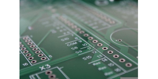
Solder Mask refers to the printing of solder mask ink on the surface of the PCB where soldering is not required. Due to the fluidity of solder paste at high temperatures when soldering printed circuit boards. Therefore, a layer of solder resist must be printed where soldering is not required to prevent the solder paste from flowing and overflowing and causing short circuits. It is an epoxy or photoimaging polymer layer used to protect copper on the PCB surface to prevent welding. The solder mask layer covers exposed copper traces on the surface of the printed circuit board. A solder mask acts as a PCB insulation, preventing corrosion, oxidation, or damage from chemical exposure. And modern printed circuit boards have very thin and fine pitch tracks and component pins that can cause short circuits after the soldering process. By using solder resist, this problem can be prevented.What is Solder Paste Mask
Paste Mask Layer is used to make the stencil with punching holes, and the holes in the stencil correspond to the solder joints of the SMD devices on the printed circuit board. This is to help the device be soldered on the PCB, and the size of the Paste mask is the same as the size of the pads.
When soldering surface mount devices, first cover the stencil on the printed circuit board (corresponding to the pads on the actual PCB), then print the solder paste, and then scrape off the excess solder paste with a blade, and finally remove the steel sheet. In this way, the solder paste is added to the pad of the SMD device, and then the SMD device is attached to the solder paste, and finally, the soldering of the SMD device is completed by a reflow soldering machine.
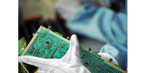
AiPCBA is an Intelligent Electronic Manufacturing Service company which can offer one-stop service from PCB manufacturing, BOM sourcing, PCB assembly, SMT, THT, PCBA testing, product assembly, packaging, and delivery.
We have over 7 years of knowledge and combined experience in rendering high tech PCB assembly service, PCB manufacturing service and different PCB assembly technologies like Through-hole (THT) and Surface Mount (SMT). Mainly, we work with three types of printed circuit boards including Rigid PCB, Flexible PCB and metal core PCB.
All PCBs in AiPCBA are produced based on UL and ISO certification standards. All our normal specification PCBs are strictly obeying to IPC-A-6011/6012 Class 2 latest version and IPC-A-600 Class 2 latest version.
Learn more about AiPCBA Turnkey PCB Assembly Service.
The data design for Solder Mask Layer and Solder Paste Mask Layer
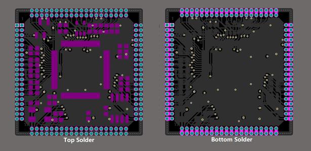
Solder Mask Layer: Solder mask can be divided into top layers and bottom There are two layers. The solder layer is to expose the pad, so the small circle or square ring seen when only the solder layer is displayed is generally larger than the pad (that is, the solder mask is used to coat the solder paste such as green oil to prevent the solder from being contaminated in the places that do not need to be welded. This layer will expose all the pads to be welded, and the opening will be larger than the actual pad). when generating the Gerber file, the small circle or square ring will be larger than the actual pad. You can observe the actual effect of solder layers.Solder Paste Mask Layer: Usually, the size of the aperture on the steel film is smaller than the actual soldering on the circuit board. By specifying an expansion rule, the solder paste protective layer can be enlarged or reduced. For different requirements of different pads, multiple rules can also be set in the solder paste protection layer.
The Difference between Solder Mask and Paste Mask
(1)Different functionsSolder Mask: The solder mask layer is a window on the whole surface of solder mask green oil (or other colors of ink), the purpose is to allow soldering, by default, the area without solder mask layer should be green oil.
Solder Paste Mask: The solder Paste Mask layer is used to make the stencil, and the stencil can accurately place the solder paste on the patch pads that need to be soldered, which is used for the package of the SMT.
(2)Different production processes
Solder Mask process: Solder mask material must be used by liquid wet process or dry film lamination.
Dry film solder mask material is supplied in 0.07-0.1mm (0.03-0.04″) thickness and may be suitable for some surface mount products, but this material is not recommended for fine pitch applications. Generally, solder mask openings should be wider than The pads are 0.15mm (0.006″) larger. This allows a 0.07mm (0.003") gap on all sides of the pad.
Low profile liquid photosolder resist is economical and often specified for surface mount applications, providing precise feature size and clearance.
Solder Paste Mask: process is made by chemical etching, laser cutting, and electroform.
Chemical etch - data file PCB → film production → exposure → development → etching → steel sheet cleaning → netting.
Laser cutting - film making → taking coordinates → data file → data processing → laser cutting → grinding → netting.
Electroforming method (electroform) - coating photosensitive film on the substrate → exposure → development → electroforming nickel → forming → steel sheet cleaning → netting.
PCB manufacturing and PCB Assembly in AiPCBA
AiPCBA is providing PCB manufacturing and PCB assembly services. We have clients from different industries all over the world. We can provide services from PCB layout to PCB prototyping, volume manufacturing, PCB assembly, and electronic box assembly. Our Printed Circuit Boards are used in robotics, medical, automotive, communications, industrial, and consumer electronics. Well suited to our client’s requirements in terms of cost-effectiveness, quality, delivery, and any other requirements. All PCBs in AiPCBA are produced based on UL and ISO certification standards. All our normal specification PCBs are strictly obeying to IPC-A-6011/6012 Class 2 latest version and IPC-A-600 Class 2 latest version.
AiPCBA’s advantage of PCB manufacturing and Assembly
AiPCBA's one-stop PCBA service, save you worry and energy: The most basic advantage is high efficiency and low cost. You don't need to purchase materials by yourself, you don't need to manage PCBA production projects by yourself, and you don't need to connect with multiple suppliers. You only need to safely hand over the production data to AiPCBA, and you can get your PCBA circuit board in about a week.
Efficiency advantages of resource centralization: AiPCBA focuses on improving the parts sourcing, PCB manufacturing, and PCBA processing capabilities of PCBA manufacturing, and improving the efficiency of all aspects of production. Various components and materials of PCBA products are collected and delivered in one factory, which can reduce the confirmation link of multiple inventory materials for back-and-forth delivery and receipt of component materials, which can save more than 3 days. Most of the passive components of your product can be directly called from the AiPCBA factory warehouse, and these materials can be flexibly deployed directly on the SMT production line, without considering the minimum packaging problem of material procurement, saving procurement time.
The Cost advantage of one-stop service: Your PCBA project will be produced by AiPCBA. AiPCBA's resources in all aspects are very concentrated, which will save you a lot of time in all aspects of PCBA production, shorten product delivery, help you avoid various material supply chain risks and manufacturing ability risks in advance, and can help you advance your product launch process and catch the business opportunities.
Learn more about AiPCBA Turnkey PCB Assembly Service.
How to get the Quote in AiPCBA
PCB quote: In our online PCB quotation system, you only need to upload the Gerber file and fill in the PCB specifications, you can easily get a quotation within 10 seconds. At the same time, our quotation page is also equipped with the function of an online Gerber 3D Preview. you can upload a Gerber file and have a 360-degree view of your PCB design.
BOM quote: AiPCBA's self-developed BOM quotation system can identify component information within 30 seconds, and analyze and quote market prices. And our BOM quotation system does not have strict requirements on the BOM format, all of which are based on the development of our strong R&D team, and play an extremely important role in our thousands of BOM price confirmations.
PCB Assembly Quote: Based on AiPCBA's PCB and BOM online quote system, we have also developed the calculation formula for assembly costs accordingly and combined these three quotation systems to form our complete one-stop PCBA quotation. As long as you upload the Gerber file and BOM list, our system will give you a complete PCBA quotation within 30 seconds.
AiPCBA also accepts Requests for a quotation by email, we are glad to receive your attachments (Gerber files, BOM list, etc. ) Pls feel free to contact us at sales@aipcba.com.