From the 20th century to the early 21st century, the circuit board electronics industry has developed rapidly in technology, and electronic technology has been rapidly improved. As the printed circuit board industry, only with its synchronous development can we continuously meet the needs of customers. With the small size, light weight and thinness of electronic products, printed circuit boards have developed flexible boards, rigid-flex boards, blind buried via circuit boards and so on.
When it comes to blind holes or buried holes, first of all, we start with the traditional multilayer board. The structure of the standard multi-layer circuit board is composed of the inner layer circuit and the outer layer circuit, and then uses the drilling process and the metallization process in the hole to achieve the internal connection function of each layer circuit. But because of the increase in circuit density, the packaging methods of parts are constantly updated. In order to allow a limited circuit board area to be able to place more high-performance parts, in addition to the thinner the line width, the aperture is also reduced from the DIP jack aperture 1 mm to SMD 0.6 mm, and further reduced to 0.4mm or less. However, it still occupies the surface area, so there are buried holes and blind holes.
1) Buried Via
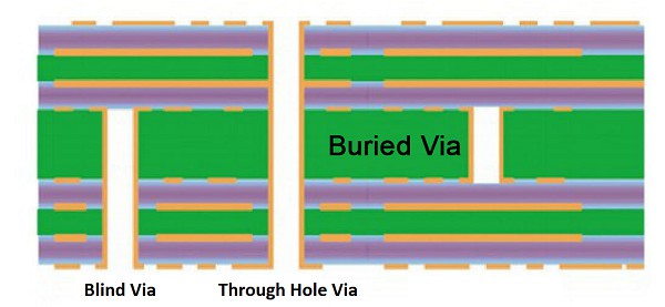
Blind vias are copper-plated vias that are only interconnected with an outer layer of the PCB. However, it is important to know that the hole does not reach the circuit board all the time, making it "blind" or "invisible" to the naked eye. The through holes between the inner layers cannot be seen after being pressed, so there is no need to occupy the area of the outer layer. The upper and lower sides of the hole are in the inner layer of the board, in other words, they are buried inside the board. The hole of the blind hole must be defined with a separate drill file, and the ratio of the hole diameter to the drill bit diameter must be less than or equal to 1. Each hole has an inner layer. The smaller the hole, the smaller the distance between the outer layer and the corresponding inner layer.
2) Blind via
The buried via connects at least two layers without reaching the outer edge of the board. Therefore, it is buried inside the circuit and completely inside. Applied to the connection between the surface layer and one or more inner layers, one side of the hole is on one side of the board, and then it reaches the inside of the board. Because these buried vias are used to connect different parts of the inner layer of the prototype circuit board, each hole must be made from a separate drilling file.
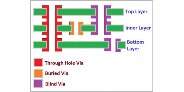
High-density multilayer printed circuit boards may generally have micropores. The blind hole is only exposed on one side of the board, while the buried hole connects the inner layer without being exposed on any surface. Blind holes and buried vias are used to connect the PCB layer, and the PCB layer space is very superior. Blind vias connect the outer layer to one or more inner layers, but do not pass through the entire board. The buried via connects two or more inner layers, but does not pass through the outer layer.
Generally speaking, these two types of vias are used for higher density circuit boards because simple circuit boards do not actually require different design structures because they consist of only one layer.