HDI Boards Process
Posted: May 14, 2022
By: Bonnie
A circuit board which has a higher wiring density per unit area as opposed to conventional board is called as HDI PCB. They have finer lines and spaces, smaller vias and capture pads and higher connection pad density than employed in conventional PCB technology.
Contents
1. What is a 4 layer PCB?
2. What is a PCB stackup?
3. What is sequential lamination?
4. What is a blind via?
5. HDI PCB market
1. What is a 4 layer HDI PCB?
The 4-layer PCB stackup, on the other hand, is quite elaborate. Two inner layers, inner layer 1 and 2, are sandwiched between the top and bottom layers. From top to bottom, the 4-layer PCB stackup goes something like this: ... A core sublayer is part of inner layer 1, which has a width of 0.037 in.
2. What is a PCB stackup of HDI?
The PCB stackup is the substrate upon which all design components are assembled. A poorly designed PCB stackup with inappropriately selected materials can degrade the electrical performance of signal transmission, power delivery, manufacturability, and long term reliability of the finished product.
3. What is sequential lamination of HDI PCB?
Lamination is the process by which the core(s) of a printed circuit board (PCB) are melted together through heat and pressure with copper layers and prepreg layers (in multi-layer PCBs).
Sequential lamination is a variety of technologies, where already laminated subparts (or subcomposites) are laminated to additional layer of copper, or another subpart. A sequentially-laminated Printed Circuit Board (PCB) goes through at least two lamination cycles, and can go through many more.
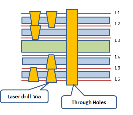
4. What is a blind via for HDI PCB?
Blind and buried vias are used to connect between layers of a PCB where space is at a premium. A Blind Via connects an outer layer to one or more inner layers but does not go through the entire board. A Buried Via connects two or more inner layers but does not go through to an outer layer.
5. HDI PCB market
HDI boards, one of the fastest growing technologies in PCBs, are now available at AiPCBA. HDI Boards contain blind and/or buried vias and often contain microvias of .006 or less in diameter. They have a higher circuitry density than traditional circuit boards.
More resources:
Do you have any questions about the above-mentioned? Contact us now, we will reply to you soon.
Is the article useful to you?
No
Yes(
8
)
8
8230
1
Share to: