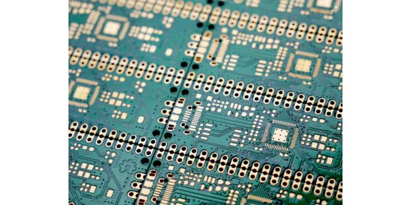
What is Multilayer PCB?
PCB can be divided into single-sided, double-sided, and multi-layered boards from the structure.
The Features of Multilayer PCB
The biggest difference between a multilayer PCB and a single-sided or double-sided PCB is the addition of an internal power layer and a ground layer. The power line and ground network are mainly arranged on the inner electrical layer.
However, the circuit layout of multilayer PCB is mainly based on the top and bottom layers, supplemented by the middle circuit layer. Therefore, the design of a multi-layer PCB is basically the same as that of a double-sided PCB.
AiPCBA is a reliable multilayer PCB manufacturer and one of the cheapest multilayer PCB manufacturers. With advanced PCB manufacturing capabilities, AiPCBA provides various multi-layer PCBs, such as rigid-flex PCB, flexible PCB, high-speed PCB, HDI PCB, etc.
The Advantages of Multilayer PCB
Multilayer PCB has many advantages, such as high assembly density, small size; a shortened connection between electronic components, fast signal transmission speed, convenient circuit layout; good shielding effect, and so on.
1) Small size: The small size makes these PCB very important because the size of the technology is getting smaller and smaller with electrical and electronic devices. The multilayer design of PCB provides a smaller size for electronics and electronic devices such as computers, smartphones, tablets, wearables, and laptops, etc.
2) Good quality: A key characteristic of this type of PCB is its quality, these multi-layer printed circuit boards are used very well and have no problems throughout their service life.
3) Durability: Multilayer PCB are durable because they can withstand not only enormous weights but also high temperatures. There is always insulation between the different layers in these PCB to provide protection from damage.
4) Flexible design: Larger circuit layout space.
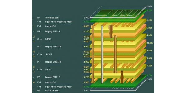
The Layer Structure of Multilayer PCB
The Layers Structure of Multilayer PCB is mainly composed of the following layers: Copper foil, Core, Prepreg, Solder resist, Character ink, and Surface treatment materials. Learn more about the AiPCBA PCB Capabilities now!
The Multilayer PCB Manufacturing Process
1.CUTTING
Cutting is the process of cutting the original copper-clad board into a board that can be made on the production line. Generally, the purchased materials come in the following sizes: 36.5 INCH × 48.5 INCH, 40.5INCH X 48.5 INCH, 42.5 INCH X 48.5 INCH, etc. PCB design engineers and PCB production engineers always consider how to maximize the use of PCB raw materials throughout the process.2.INNER DRY FILM
The inner dry film is the process of transferring the inner circuit pattern to the PCB board.
In PCB production, we will mention the concept of graphics transfer, because the production of conductive graphics is the foundation of PCB production. Therefore, the graphics transfer process is very important for PCB production.
The inner layer dry film includes multiple processes such as inner layer sticking, exposure and development, and inner layer etching. The inner film is a special photosensitive film on the surface of the copper plate. This film will cure when exposed to light, forming a protective film on the board. Exposure development is to expose the board to which the film is attached. The light-transmitting part is cured, and the part that does not transmit light is still a dry film. Then, after development, the uncured dry film is removed, and the board with the cured protective film is etched. After the film removal process, the inner circuit pattern is transferred to the board.
3.BLACK OXIDATION
The purpose of blackening and browning:
1) Remove contaminants such as oil and impurities on the surface;
2) Increase the specific surface of the copper foil, thereby increasing the contact area with the resin, which is conducive to the full diffusion of the resin and the formation of a larger bonding force;
3) Make the non-polar copper surface into the surface with polar CuO and Cu2O, increase the polar bond between the copper foil and the resin;
4) The oxidized surface is not affected by moisture at high temperatures, reducing the chance of delamination of copper foil and resin.
4.LAMINATION
Lamination is the process of bonding layers of circuits into a whole by means of B-stage prepreg. This bonding is achieved by the interdiffusion and penetration of large molecules on the interface, which in turn interweave.
Purpose: Press the discrete multi-layer board together with the adhesive sheet into the multi-layer board with the required number of layers and thickness.
The copper foil, bonding sheet (prepreg), inner layer board, stainless steel, insulation board, kraft paper, outer layer steel plate and other materials are laminated according to the process requirements. If the board has more than six layers, it needs pre-setting.
Send the stacked circuit boards to the vacuum heat press. Using the thermal energy provided by the machine, the resin in the resin sheet is melted to bond the substrate and fill the gap.
For designers, the first consideration for lamination is symmetry. Because the board will be affected by pressure and temperature during the lamination process, there will be stress in the board after lamination. Therefore, if the laminated board is uneven on both sides, the stress on the two sides is different, causing the board to bend to one side, greatly affecting the performance of the PCB.
In addition, even on the same plane, if the distribution of copper is uneven, it will cause the resin flow rate at each point to be different, so that the thickness of the place where the copper is less will be slightly thinner, and the thickness where the copper is more will be slightly thicker. some.
5.MECHANICAL DRILLING
Mechanical drilling is to use a drill to cut at high speed to form a through hole on the PCB.
6.METALLIZE THE THROUGH HOLE
The substrate of the circuit board is composed of copper foil, glass fiber, and epoxy resin. In the manufacturing process, the cross-section of the hole wall after the substrate is drilled is composed of the above three parts.
The metallization of the hole is to solve the problem of covering the cross-section with a uniform, thermal shock-resistant metal copper.
The process is divided into three parts: one for the decontamination process, two for the chemical plating through-hole process, and three for the thickening copper process.
The metallization of holes involves a concept of capability, thickness-to-diameter ratio. Thickness-diameter ratio refers to the ratio of plate thickness to aperture. When the board is getting thicker and the pore size is continuously decreasing, it is more and more difficult for the chemical liquid to enter the depth of the drill hole. A thin coating is still inevitable. At this time, there will be a slight open circuit in the drilled layer. When the voltage is increased and the board is impacted under various harsh conditions, the defects are completely exposed, causing the board circuit to be broken, and the specified work cannot be completed.
7.DRY FILM & PATTERN PLATING
The outer layer graphics transfer is similar in principle to the inner layer graphics transfer. Both use photosensitive dry film and photographic methods to print circuit patterns on the board. The difference between the outer dry film and the inner dry film is:
1) If the subtraction method is used, the outer dry film is the same as the inner dry film, and the negative film is used as the plate. The part of the cured dry film on the board is the circuit. The uncured film is removed, the film is removed after acid etching, and the circuit pattern is left on the board because it is protected by the film.
8.WET FILM SOLDER MASK
The solder mask process is to add a layer of solder mask on the surface of the board. This layer of solder mask is called Solder Mask or Solder Mask Ink, commonly known as a green oil. Its role is mainly to prevent undue tin on conductor lines, etc., prevent short circuits between lines due to moisture, chemicals, etc., disconnection, insulation caused by bad operations during production and assembly, and resistance to various harsh environments Printed board functions, etc.
At present, this layer of ink used by PCB manufacturers basically uses liquid photosensitive ink. Its production principle is partially similar to that of circuit pattern transfer. It also uses film to block the exposure and transfer the solder mask pattern to the PCB surface.
The specific process is as follows: Pre-treatment-> coating one> pre-bake-> exposure-> development-> UV curing-> thermal curing.
Associated with this process is the solder mask file, which involves process capabilities including solder mask alignment accuracy, green oil bridge size, fabrication methods, solder mask thickness, and other parameters. At the same time, the quality of solder resists ink will also have a great impact on the later surface treatment, SMT placement, preservation, and service life. Coupled with its long production time and many production methods, it is an important process in PCB production.
9.SILKSCREEN
Because the character accuracy requirements are lower than that of wiring and solder mask, the characters on the PCB are basically screen printed. In the process, the screen for the printing plate is first produced according to the character film, and then the character ink is printed on the plate using the screen, and finally, the ink is dried.
10.SURFACE FINISHED
PCB surface finish refers to the process of artificially forming a surface layer with different mechanical, physical and chemical properties of the substrate on the components and electrical connection points of the PCB. If the surface treatment of the circuit board is not carried out, it will be easy to form false welding and virtual welding. In severe cases, the pads and components cannot be welded. The purpose of surface treatment is to ensure good solderability or electrical performance of the PCB.
11.Profiling
So far, the PCB we have produced has always been in the form of a PANEL, that is, a large board. Now that the production of the entire board has been completed, we need to separate the delivery graphics from the big board according to (UNIT delivery or SET delivery). At this time, we will use the CNC machine tool to process in accordance with the pre-programmed program. The contour edge and strip milling will be completed in this step. If there is a V-CUT, the V-CUT process needs to be added. The capacity parameters involved in this process are shape tolerance, chamfer size, and inner corner size. The safety distance between the figure and the edge of the board must also be considered during the design.
12.E-TEST
The electronic test is the electrical performance test of the PCB, which is usually also called the "on" and "off" test of the PCB. Among the electrical test methods used by PCB manufacturers, needle bed test and flying probe test are the most commonly used.
1) Needle beds are divided into general network needle beds and special needle beds. The universal needle bed can be used to measure PCBs with different network structures, but its equipment is relatively expensive. The dedicated needle bed is a needle bed specially formulated for a certain PCB, and it is only applicable to the corresponding PCB
2) Flying probe test uses a flying probe test machine, which tests the continuity of each network separately by moving probes (multiple pairs) on both sides. Since the probes can move freely, the flying probe test is also a general test.
13.Final inspection
Inspection methods usually include:
1)Optical inspection: It is a device that detects common defects encountered in welding production based on optical principles. AOI is a new type of testing technology emerging, but it is developing rapidly, and many manufacturers have launched AOI testing equipment. When automatic detection, the machine automatically scans the PCB through the camera, collects the image, compares the solder joints tested with the qualified parameters in the database, after image processing, checks out the defects on the PCB, and displays / marks the defects through the display or automatic sign Come out for repair by maintenance personnel.
2) Target inspection confirmation: visual inspection confirmation to confirm or eliminate some true and false defects.
3) Visual inspection: repair or scrap the confirmed defects, and classify the different layers.
14.Package
The main packaging types are Anti-Static Packaging, Moisture-Proof Packaging, and Anti-Vibration Packaging, but the usual packaging only uses vacuum packaging.AiPCBA Intelligent Manufacturing Technology (Shenzhen) Co., Ltd. focuses on one-stop PCBA intelligent manufacturing services, using artificial intelligence and big data technology, independently developed China's first PCBA flexible intelligent manufacturing platform AiPCBA®, integrating electronic components supply, product prototype, trial production, volume production, to provide customers with high-quality, high-efficiency quality services.