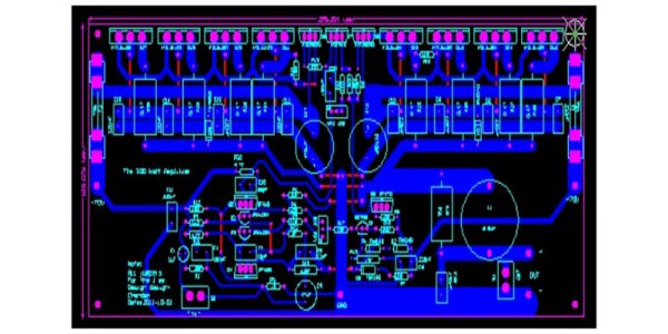
1).Gerber file is a file that can be produced by all circuit design software. It is also known as stencil data in the electronic assembly industry and light drawing file in the PCB manufacturing industry. Gerber files are arguably the most versatile and extensive file format in the electronic assembly industry. Therefore, for an electronic manufacturing enterprise, it is very important to have a computer-aided manufacturing CAM software that can process Gerber files, which can assist in the preparation, manufacturing and testing of product production.
2).Gerber file is the standard format of EIA, which is divided into rs274-d and rs274-x, among which rs274-x is the extension file of rs274-d. Where conditions permit, the manufacturing department shall, to the extent possible, require the user or design department to provide the Gerber document of rs274-x, which is conducive to the production preparation of each process.
3).CAD documents generally refer to original PCB design documents, such as protel, PADS and other PCB design documents, while users or enterprise design departments are usually only willing to provide Gerber files for PCB production and manufacturing departments for various considerations.
4).GERBER has two formats:
(1).RS274D contains XY DATA and does not contain d-code file. The client shall provide the corresponding d-code file.
(2).RS274X contains XY DATA, and d-code is also defined in this file.
(3). D - CODE file (APERTURE LIST) for ASC Ⅱ text format, it defines the D - CODE size, shape and exposure of the way.

PCB manufacturing principle:
We open the universal computer disc can see a soft film (flexible insulation substrate), printed on the white (silver paste) conductive graphics and position graphics. Because this pattern is obtained by the universal screen printing method, we call this printed circuit board flexible silver paste printed circuit board. The same is true of the computer motherboards, graphics CARDS, network CARDS, modems, sound CARDS and printed circuit boards on home appliances that we see in the computer city. The substrate used is made of paper base (commonly used on one side) or glass base (often used on both sides and in multiple layers), preimpregnated with phenolic or epoxy resin, and coated with copper sheets on one or both sides of the surface and then laminated. This circuit board copper-clad sheet, we call it a rigid board. And then we make printed circuit board, we call it rigid printed circuit board. Single-sided printed circuit board we call single-sided printed circuit board, double-sided printed circuit board with printed circuit board, and then through the hole of the metalization of double-sided interconnection formed printed circuit board, we call it double panel. If using a double lining, two one-way for outer layer or two double lining, two blocks of single outer layer of the printed circuit board, through the positioning system and alternate insulation adhesive materials and conductive graphics interconnection according to design requirement of printed circuit board becomes four, six layer printed circuit board, also known as multilayer printed circuit board. There are now more than 100 layers of functional PCB.

PCB manufacturing process:
1) The production process of PCB is relatively complex, involving a wide range of processes, from simple mechanical processing to complex mechanical processing, including common chemical reactions, photochemical electrochemical thermochemical processes, computer-aided design CAM and other aspects of knowledge. And in the process of production process problems and will always meet new problems and some problems in didn't find out the reason disappears, because its production process is a kind of continuous line form, a link any problems will be caused production across the board or the consequences of a large number of scrap, PCB, if there is no recycling scrap process engineers working pressure is bigger, so many engineers left the industry to the PCB equipment or material do the work of sales and technical services.
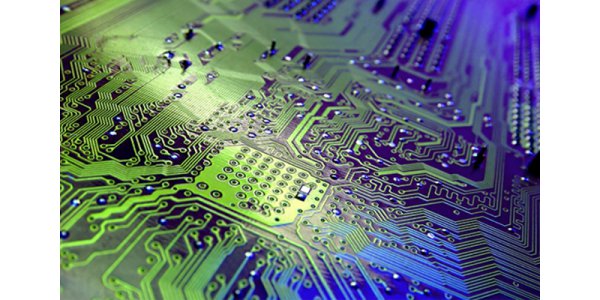
2). The base board of the board itself is by the material of insulation and heat insulation, and is not easy to bend into. On the surface can see the fine line material is copper foil, originally copper foil is covered in across the board, and to get rid of the central in the manufacturing process of etching, stay part to turn into a network of fine lines. The lines are known as wire (conductor pattern) or the wiring, and used to provide the PCB components of the circuit connection.
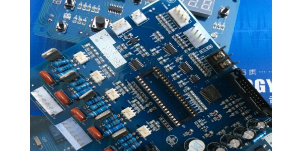
3). In order to secure components on PCB, we will their feet directly welding on the wiring. In the most basic on the PCB (single panel) of parts are concentrated in one Side, the wires were focused on the other Side. So we need to make holes in the board, so that his feet through to the other Side to the board, so parts of the foot is welded on the other Side. Because of this, the face of positive and negative of PCB respectively called parts surface (Component Side) and the welding surface (Solder Side).
4). If there are some parts on the PCB, which can be removed or put back after the production is completed, the Socket will be used for the installation of this part. Since the Socket is directly welded to the board, the parts can be disassembled at will.
5). If you would have two pieces of PCB interconnected, normally we would use commonly known as the "golden finger" edge connectors (edge connector). Gold finger contains many bare copper pad, the copper pad in fact is a part of the PCB wiring. Usually connection, we will be one of the gold finger on a piece of PCB into another piece of PCB on the appropriate Slot on (commonly called expansion Slot Slot.) in a computer, like a display card, sound card, or other similar interface card, is through the gold finger to connect to the motherboard.

6). Green or brown on the PCB, is resistance welding paint (solder mask) color. This layer is the protective layer of insulation, can protect copper wire, can also prevent the parts are welded to the right places. On the solder resist layer and will be printed on a layer of silk screen printing (silk screen), usually in the above will be printed on words and symbols (mostly white), to indicate the location of the various parts on the board. Screen printing surface is also known as icon (legend).
7).PCB etches the copper wire of the complex circuit between parts on a board after careful and orderly planning, providing the main support body for the installation and interconnection of electronic components. It is an indispensable basic part of all electronic products.
PCB a flat plate made of a nonconductive material on which chips and other electronic components are usually predrilled. The holes in the components help to electronically connect pre-defined metal paths printed on the surface of the board, pass the pins of the electronic components through the PCB, and then attach a conductive metal electrode to the PCB to form a circuit.
