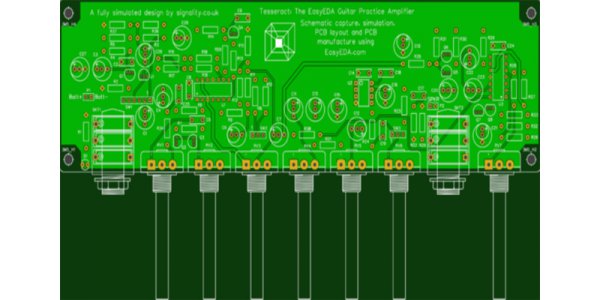
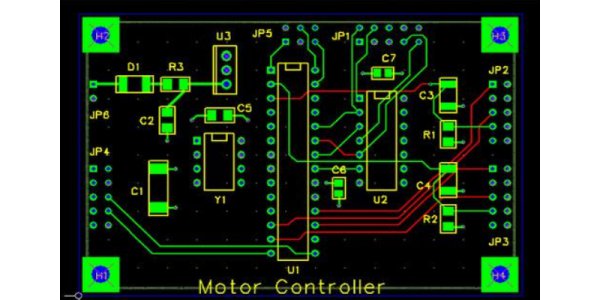
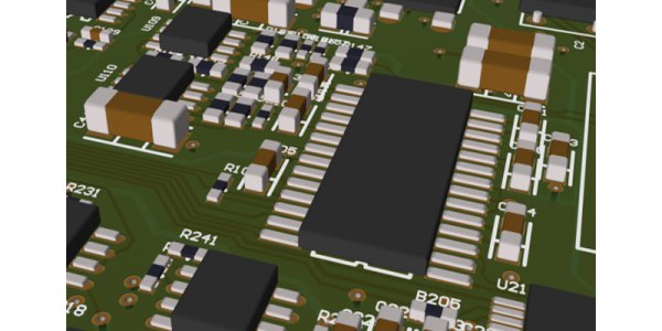
Gerber, also known as "light drawing", usually represents only one format such as rs-274, 274D, 274X, etc., which serves as the two media to convert the graphic data of the design into PCB manufacturing, namely a cad-cam data conversion format specification. The important use is the PCB layout drawing, finally by the PCB manufacturer to complete the PCB manufacturing. Regardless of the CAD odds and ends, the external CAD database must eventually be converted to a GERBER file. In this process, Aperture table represents the lens size, shape, and status information of the plotter. The transformation between the two is usually tangible, and once the Gerber occurs, the plotter can start the task. The plotter is an expensive but accurate device that can be accurate to less than 1mil.
1).The rs-274-d was developed in 1985 in accordance with the EIA rs-274-d specification code, and its material content includes the word address material and the parameter file and control code of the plotter. Gerber in this format must include a Aperture File, which means that Gerber File and Aperture File are separate files. The rs-274-d has been used for countless years now. Since the evolution of electronic products has already exceeded the current needs, the original rs-274-d format has gradually been insufficient to be used, which has been replaced by the enhanced rs-274-x.
2).rs-274-x occurred in 1992, which is the most popular material format today. It is an extended version of rs-274-d based on rs-274-d. Aperture of rs-274-x format is integrated into Gerber File, i.e., "containing D code".
In addition to the above, there are a few data format specifications in use or development, such as MDA/Fire9000 and Barco DPF, which are not very commonly used and will not be detailed here.
Gerber Format is a common material Format among the electronics industry, which is used for the design and production of PCB on both ends of the body, just like the civil or mechanical hardware industry commonly used AutoCad software input DXF or HPGL Format is common, is the designer of the design of documents and other pieces of links.

3) Aperture File description:
(1) the lens File mainly describes the shape and size of the lens used by Gerber File;
Aperture File + Gerber File = intact PCB Layout;
(2) common field: D_CODE: D code, namely lens number; The SHAPE of the lens; SIZE: the SIZE of the lens;
4). Common borehole and its meaning:
(1)PTH-- a hole coated with metal to connect the conductive pattern of two layers or outer layers;
(2)NPTH-- non-plated through hole, hole wall is not coated with metal but used for mechanical devices or mechanical fixed components;
(3)VIA-- through hole, which is used for the electrical connection between conductive figures in different layers of printed board (such as embedded hole, blind hole, etc.), but cannot be inserted into the plating through hole of component guide leg or other reinforcing data;
(4) blind hole -- a conducting hole extending to only one outer surface of the printed board;
(5) buried hole -- a conducting hole not extending to the appearance of the printed board.
5). Polarity description of Gerber File:
(1) Positive: Gerber depicted the line layer, and the figure depicted was mainly copper; Or Gerber describes the resistance layer, and the figure is important to describe the anti-welding part (that is, the ink);
(2) Negative: Gerber depicted the line layer, and the figure depicted was important because there was no copper part; Or Gerber describes the layer of resistance to welding, and the graph is important to describe the non-resistance to welding (that is, do not cover the ink);
(3) Compostive: the layers depicted by Gerber are decomposed by different polarity layers. It is usually a layer cut and a positive polarity superposition. The polarity of the cut layer is c, which plays an important role in line protection or additional materials.

Gerber layers:
1).LAYER: the wiring LAYER is copper foil wiring. ;
2).SILKSCREEN layer, very easy to understand, printed things such as text;
3).Solder mask: solder the green oil layer, which refers to the part of the board to be covered with green oil; Because it is a negative output, so actually part of the actual effect of the soldermask is not green oil, but tin, silver!
Paste mask: paste paste layer and welding aid layer are used for machine mounting. They are the pads corresponding to all mounting elements. The size is the same as that of toplayer/bottomlayer, and they are used for tin leakage in steel mesh.
Of course, there is also a mechanical layer, such as the irregular shape of the plate frame.
5).Tin or gold plating:
"Solder layer corresponding to the copper layer is copper would tin plating or gold plated" this sentence is a person who work in the production of PCB factory said, his meaning is: if you want to make the painting in the part of solder layer made of the effect is tin plating, a copper sheet part then the corresponding solder layer (i.e., and solder layer corresponding area have the toplayer or bottomlayer)! Solder layer indicates the area not covered with green oil!
6).Difference between Soldermask and paste mask:
Paste mask industry commonly known as "steel mesh" or "steel plate." This layer does not exist on the printed board, but is a separate sheet of steel with the SMD pads hollowed out in place. General hollowed-out shape and SMD welding pad, slightly smaller size. This steel mesh is used in SMD automatic assembly welding process to apply tin paste on SMD welding pad. In other words, PASTE MASK is only used for the mounter, and no additional processing is done on the PCB.
7).NC Drill refers to the data that Pads output to input into the CNC drilling machine, including coordinates, hole size and other information, which can be directly input into the CNC for processing after a simple edit. Therefore, this file is usually for the PCB processing plant.
Drill Drawing, description of the hole size of the welding pad and the hole through the hole. Is the output of the d-code table file, now the general format is RS274, usually for the chip machine.

