Introduction
In high frequency PCB design, the power supply is designed as a layer, in most cases much better than a bus, so that the circuit can always follow the path with the least impedance. In addition, the power board must provide a signal circuit for all generated and received signals on the PCB, which minimizes the signal circuit and thus reduces noise. This point is often overlooked by low-frequency circuit designers.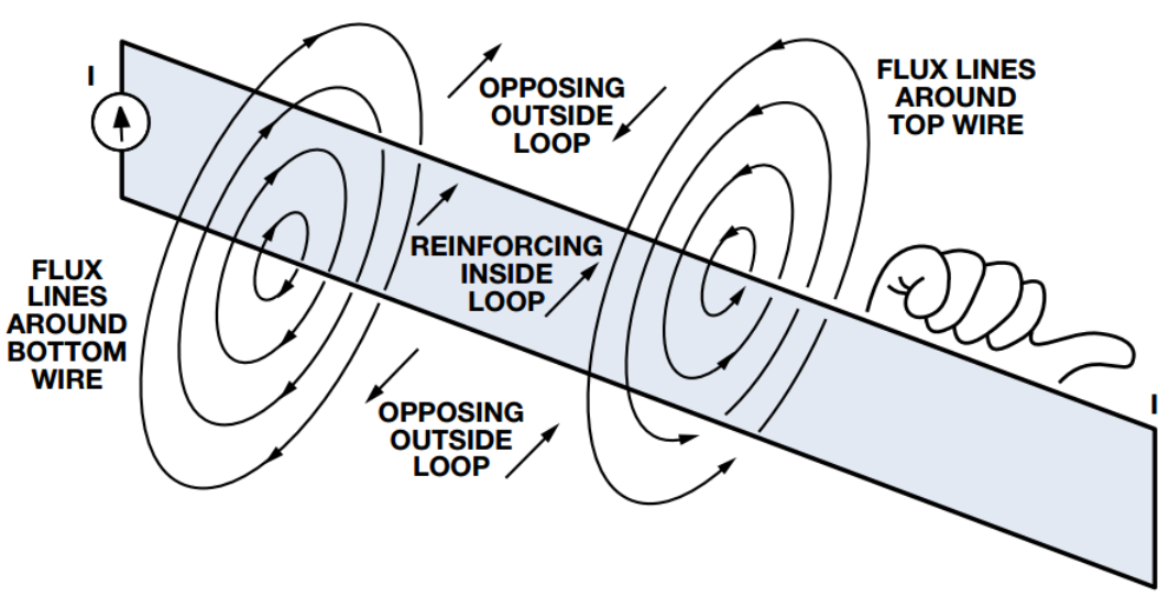
1.0 Composition of high frequency PCB:
-Solder side: metal hole for welding components.-Via hole: there are two types of metal via hole and non-metal. Metal is used mainly to connect the components of the layers.
-Installation hole: used for fixed circuit board.
-Conductor trace line: electrical network copper film used to connect the components of the components.
-Connector: the components that are used between the circuit boards.
-Fill: copper applied to the ground line network can effectively reduce the impedance.
-Electrical boundary: to determine the size of the circuit board, all the components on the board cannot exceed the boundary.
2.0 Components layout
When making high frequency PCB board, the designer should first consider the electrical performance between components. Only when the electrical properties of the PCB meet the requirements can the designer consider the convenience of wiring and other properties of the PCB.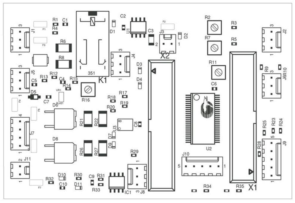
2.1 The electrical property
In the layout, the designer should make the components to close electrical relationship as close as possible, especially for the wiring between some components with high frequency. Because the connection between these components is relatively short. For high-power devices, the layout should be separated from some small signal devices to reduce the interference to small signal devices. Then, if the system is composed of multiple PCB boards, high-speed devices with these characteristics should be placed on the same PCB board as far as possible. It avoids the problem of shift errors to cause the unequal clock signal transmission delay time between the main PCB board and different plug-in boards.
For example: In the layout of high-speed Ethernet, the anti-interference resistance capacitance of Ethernet chip DM9000 and PH163539 should be attached around the core chip as far as possible.
2.2 Routing
2.2.1 Basic principles of routing:
- Unified and stable between power supply and ground.
- Carefully considered routing and proper terminations can eliminate reflections.
- Carefully considered routing and proper terminations can reduce capacitive and inductive crosstalk.
- Suppress noise to meet EMC requirements.
2.2.2 Ground wire and Volt current condenser
If the ground wire or power supply layout on a high frequency PCB is not reasonable, the PCB will produce electromagnetic interference. It means that the high frequency PCB performance will be degradation. Worse still, the PCB might just stop working.
There is an equation for gap capacitance between ground and power supply:
![]()
Xc-Capacitance reactance, ω-Pin frequency,f-signal frequency,C-capacitance(farad)
It can be seen from the equation, the greater the gap capacitance between the ground and the power supply, the less its capacitance resistance will be, and at the same time, it will produce noise interference.
Methods to reduce noise between ground and power supply:
(1) Increase line width and reduce noise.
(2) Common ground processing to reduce modulus interference.
(3) Conduct signal wire wiring on the power supply or ground wire layer.
2.3 Material requirements
1. Dissipation factor (Df) must be small (and stable)
2. Dielectric constant (DK) must be small (and stable)
3. Low water absorption
4. The thermal expansion coefficient of copper foil should be as close as possible
5. Heat resistance, chemical resistance, impact strength and peel strength shall be maintained in good condition.
3.0 High frequency PCB manufacturing notes
1. Impedance control requirements and relative line width control are relatively strict. Their tolerance is generally around 2%.2. As the special plate, PTH does not have a high adhesion. It is usually necessary to roughen the pores and surface with the help of plasma treatment equipment. This is to increase the adhesion of PTH copper hole and solder ink.
3. It cannot grind the plate until it has been blocked. This is because it will reduce the adhesion, so that it can only be used with a micro etching potion for coarsening.
4. Most of boards is Teflon type of materials. Therefore, this requires the use of special milling cutters, if the producer uses ordinary milling cutters, there are many rough edges on the board.
