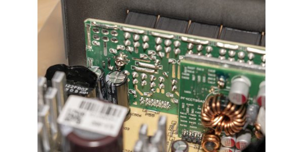
SMD components (SMD / SMC, also known as chip components) is a new type of micro-small components without leads or short leads. It is suitable for mounting on printed boards without through holes. It is based on surface mount technology (SMT). Dedicated components. Compared with traditional through-hole components, the mounting density of chip components is high, which reduces the influence of lead distribution, reduces parasitic capacitance and inductance, has good high-frequency characteristics, and enhances the ability to resist electromagnetic interference and radio frequency interference.

1. Standard parts
Part specifications:
(1) Part specifications, that is, the overall dimensions of the parts, have formed a standard part series, and each part supplier is manufactured according to this standard.
The dimensions of standard parts are expressed in English and metric.
English notation: 0805
Metric notation: 2125
meaning:
L: 0.08 inch (2.0mm) W: 0.05 inch (1.25mm)
1inch = 25.4mm.
Today the smallest standard part is 0201.
2. IC parts
Basic IC type
(1) SOP (Small outline Package): The parts have feet on both sides, and the feet are spread outward (commonly called gull-wing pin).
(2) SOJ (Small outline J-lead Package): There are feet on both sides of the part, and the feet are bent toward the bottom of the part (J pin).
(3) QFP (Quad Flat Package): There are feet on four sides of the part, and the feet of the part open outward.
(4) PLCC (Plastic Leadless Chip Carrier): There are feet on four sides of the part, and the part feet are bent toward the bottom of the part.
(5) BGA (Ball Grid Array): There are no feet on the surface of the part, and the feet are arranged in a spherical matrix at the bottom of the part.
(6) CSP (CHIP SCAL PACKAGE): Part size packaging.
IC title
3. How to solder SMD components
SMD components are the most commonly used components such as resistors, capacitors, LED lights, etc. The smaller components that we make now are basically SMD.
3.1 A typical SMD component, this component is very, very small, such as the 0603 package may be only half the size of the crescent white forefinger.
3.2 This kind of component is placed in a special patch component box, generally divided into two types 0805 and 0603, namely 08 * 05 and 06 * 03. When taking such components, use tweezers. Carefully clamp the narrow ends of the patch with tweezers and clamp it to the workbench.
3.3 The positions of the soldered components are basically two legs of one component corresponding to two pads. Replace the welding torch with a pointed welding head. After heating to 320 to 330 celsius, dip a little tin with the welding torch. Here tin does not need to be so much as in-line components.
3.4 After the solder gun is stained with tin, lightly tap on one of the two pads, spread the tin evenly on it, and swell it up a little, but it must not be directly formed into a small hill like soldering in-line resistors. Or bulging, so that too much tin will affect later work.
3.5 After completing the above steps, hold the welding gun with your right hand to ensure that the tin on the pad is still molten. Use your tweezers to pick up the chip resistor with your left hand, and push the pad from the side without tin to the side with tin to let the patch The pins of the resistor are attached to the pads and tinned.3.6 Remove the solder gun and let the tin cool down. At this time, the chip resistor is fixed on the pad. At this time, use the pad to dip some tin, and gently point on the other of the two pads, and paste the tin and the other end of the chip resistor together. After the tin is cooled, the entire chip resistor is used. The tin is firmly attached to the pad.
Note: The key is to solder one end of the chip resistor before soldering the other end.
