What is a Multilayer PCB?
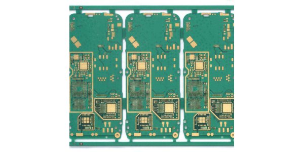
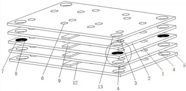
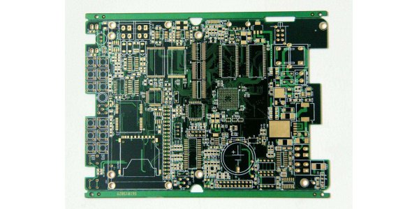
A multi-layer or multi-layer printed PCB circuit board is a PCB circuit board composed of two or more conductive layers (copper layers) stacked on each other. The copper layers are bonded together by a resin layer (prepreg). Multi-substrate is the most complex type of printed circuit board. Due to the complexity of the manufacturing process, the lower throughput and the difficulty of redoing, their prices are relatively high.

A multilayer circuit board has at least three conductive layers, two of which are on the outer surface, and the remaining layer is synthesized in an insulating board. The electrical connection between pcb circuit boards is usually achieved through plated through holes on the cross section of the circuit board. Unless otherwise stated, multilayer printed circuit boards, like double-sided boards, are generally plated through-hole boards.
Multi-substrates are manufactured by stacking two or more layers of circuits on top of each other with reliable, pre-set interconnections. Since drilling and plating were done before all the layers were rolled together, this technique violated the traditional manufacturing process from the beginning. The inner two layers are composed of traditional double panels, while the outer layers are different. They are composed of independent single panels. Before lamination, the inner substrate will be drilled, plated through-hole, pattern transferred, developed, and etched. The outer layer that is drilled is the signal layer, which is plated through in such a way that a uniform copper ring is formed on the inner edge of the via. The layers are then rolled together to form a multi-substrate, which can be interconnected (between components) using wave soldering.
Rolling may be done in a hydraulic press or in an overpressure chamber (autoclave). In hydraulic presses, the prepared materials (for pressure stacking) are placed under cold or preheated pressure (high glass transition temperature materials are placed at temperatures of 170-180°C). The glass transition temperature is the temperature at which an amorphous region of an amorphous polymer (resin) or a portion of a crystalline polymer changes from a hard, rather brittle state to a viscous, rubbery state.

What are the Advantages and Disadvantages of Mmultilayer Circuit Boards?
Advantages:
high assembly density, small size, light weight. Due to the high assembly density, the connections between components (including components) are reduced, thereby improving reliability; the number of wiring layers can be increased, which increases design flexibility; It forms a circuit with a certain impedance; it can form a high-speed transmission circuit; it can set the circuit and magnetic circuit shielding layer, and it can also set a metal core heat dissipation layer to meet the special functional needs such as shielding and heat dissipation; simple installation and high reliability.
Disadvantages:
high cost; long cycle time; high reliability detection methods are required. Multilayer printed circuits are the product of the development of electronic technology towards high speed, multifunction, large capacity and small volume. With the continuous development of electronic technology, especially the extensive and in-depth application of large-scale and ultra-large-scale integrated circuits, multilayer printed circuits are rapidly developing in the direction of high density, high precision, and high-level digitalization. Fine lines and small apertures have appeared. , Blind and buried holes, high plate thickness aperture ratio and other technologies to meet the needs of the market.
How Many Layers Can a Multilayer PCB Circuit Board Do?
In principle, the multilayer pcb circuit board can be made as many layers as possible, only the equipment capabilities can be achieved, which is very demanding on equipment. The actual situation is that half of the common cases only achieve 4-10 layers, and military special-purpose PCBs do More than 100 layers, but this is not suitable for mass production.
In 1961, the United States Hazelting Corp. released Multiplanar, which was the pioneer of the first multi-layer board development. This method is almost the same as the current method of manufacturing multi-layer boards by plated through-hole method. After Japan entered this field in 1963, various ideas and manufacturing methods related to multilayer boards have gradually spread throughout the world. As the use of transistors has entered the era of integrated circuits, and the application of computers has gradually become widespread, due to the demand for high functionality, large wiring capacity and good transmission characteristics have become the focus of multi-layer boards.

The above are some brief introductions of multi-layer pcb circuit boards. Our company has been engaged in the circuit board industry for many years. Welcome friends to communicate.
