Posted: May 14, 2022 by: NJ
When you design a PCBA project and hand it over to a turnkey PCB Assembly manufacturer to get the finished product, you might wonder how it gets made? Good processing leads to good products. Therefore, When you know more about the PCBA manufacturing process, it will help you to choose a better PCB Assembly manufacturer. Without further ado, we will dissect the whole process of the PCBA project for you.
In the past, PCB Assembly processing often refers to SMT patch and DIP plug-in two processing. Today's turnkey PCB Assembly processing process includes PCB manufacturing, components procurement, Assembly Process, three sections. Let's start with Assembly Process.
Different circuit boards have certain process differences, but the overall processing process is roughly the same. The following is the PCBA process flow chart :
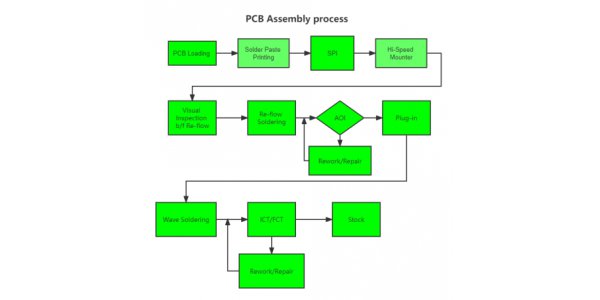
Surface Mount Process
1. Solder paste printing
The solder paste is placed on the stencil with the frame, and the solder paste is leaked onto the PCB plate by the scraper. In SMT processing, 60-70% of the quality problems occur in the solder paste printing process. To avoid the impact of solder paste quality on production, AiPCBA will have strict process management for the preservation of solder paste. And AiPCBA's advanced solder paste printing machines guarantee the quality of printing.2. SPI(Solder paste inspection)
To ensure the printing quality of solder paste, solder paste inspection is a necessary step. AiPCBA will use a solder paste thickness detector to detect solder paste printing and control the effect of solder paste printing.
3.SMT (Surface Mount)
Components are placed on Feeder, and automatic placement machines will accurately install components on the PCB plate by identifying the Pick & Place file set in advance by the engineer.This is also the most important part of SMT processing, the quality of component mounting largely depends on the performance of the SMT machine. AiPCBA automatic SMT machine from Germany EUROPLACER, its strong performance to ensure the capacity of our SMT line :
|
Item |
SMT Capabilities |
Remarks |
|
Maximum size |
900x800mm |
pcb patch size |
|
Minimum size |
20x20mm |
pcb patch size |
|
Patch size |
70x70mm Square chip |
Maximum component placement size |
|
Patch size |
01005(0.4x0.2mm) |
Minimum component placement size |
|
Patch type |
360 kinds |
|
|
CPH |
40000 |
Placement speed per hour |
|
Mounting accuracy |
±0.02mm |
|
|
Mounting minimum pitch |
0.20mm |
Equipment placement minimum spacing components |
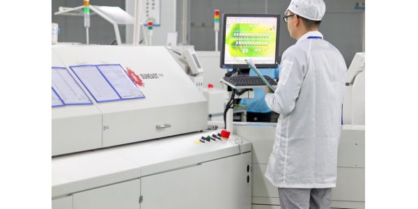
4.Reflow welding
The main function of reflow welding is to achieve SMT electronic components and PCB board welding, the following is his process principle:When the PCB enters the heating zone (dry zone), the solvent and gas in the solder paste evaporate. At the same time, the flux in the solder paste wets the pad, the end of the component and the pins, and the solder paste softens, collapses and covers the pad, the end of the component and the pins and is isolated from oxygen. When the PCB enters the insulation zone, the PCB and the component are fully preheated. To prevent PCB from suddenly entering the welding high-temperature zone and damaging PCB and components → When PCB enters the welding zone, the temperature rises rapidly so that solder paste reaches the melting state, liquid solder to the PCB pad, component end and pin wetting, diffusion, diffuse flow or backflow mixed to form solder contacts →PCB enters the cooling zone and solidifies solder joints.
5. AOI
Automatic Optic Inspection uses optical principle to detect common defects in SMT process. AOI scans PCB automatically through the camera, collects PCB images, and compares the collected PCB image data with the input parameters in the database. After simple image processing, the welding defects of PCB board are determined, and the defects are marked/displayed through the automatic marking device or equipment display, so that workers can repair in time.
6.Repair
After AOI, it is necessary to repair the circuit board with problems, such as excessive solder, solder insufficient, empty solder, open solder, missing component, floating solder, backward Part and other problems.DIP plug-in Process
1. Plug-in
The workshop staff carefully check the material model and specification according to the BOM, and then use the automatic bulk capacitor foot cutter, transistor automatic forming machine, automatic belt forming machine and other forming equipment for processing, and then insert the components into the corresponding position of the circuit board.
2. Wave soldering
After finishing the plug-in, put the PCB board into the wave welding conveyor belt, and then finish the welding of the PCB board after spraying flux, preheating, wave welding and cooling.Wave soldering is the most important part of the DIP Plug-in Process. AiPCBA has not only general wave soldering equipment but also more advanced selective wave soldering equipment, which has the following advantages compared with
general wave soldering:
- Higher welding quality, especially for prototype items.
- Higher precision, more suitable for military, medical, aerospace and other double-sided plug-in products
- The Circuit board is not easy to bend because of high-temperature deformation
- It allows for setting different parameters for each component
- It leads to cost optimization
3. Component cut foot,Repair welding and Wash the plate
- Cut the feet of the welded PCBA plate to the proper size
- Repair welding shall be carried out for the PCBA finished boards that have not been welded completely.
- Clean the residual harmful substances such as flux on PCBA products to meet the environmental protection standard cleanliness required by customers.
4. Quality inspection
The completion of assembly does not mean the completion of PCBA processing. To ensure product quality, AiPCBA will perform performance tests such as ICT, FCT, ageing test and programmed firing on PCBA according to customer requirements to ensure the normal operation of PCBA functions and reduce the later repair rate.
The above is the main process of SMT processing, next we talk about BOM procurement. Purchasing and managing BOM has always been a sore point for the industry. Each company has different BOM procurement and management modes. Here, I will analyze the component procurement and management process in PCBA from the perspective of AiPCBA.
Analyze and review BOM
When receiving the BOM from the customer, we need to check the information in the BOM first, such as whether the footprint is correct, whether the part number is complete, whether the components are out of production, and whether the parameters conflict. Most PCBA manufacturers need to manually review the BOM before feeding the EQ back to the customer. You get immediate initial feedback when you upload a BOM to AiPCBA's Analyzer. The BOM Analyzer built by AiPCBA with the help of big data can quickly analyze users' BOM, complete 90% material matching and material alternative recommendation within more than ten seconds. Meanwhile, it can also intelligently check BOM engineering evaluation, accurately check the amount of material, and give early warning of risks such as footprint error, parameter conflict, P/N selection error, and Components out of production.Purchase and quality control of components
The purchase of components can only begin after all EQs have been confirmed with the customer. The procurement channels for prototype and mass production components are different: for prototype or small batch projects, the demand for the procurement of components is quick, so they will purchase from online channels such as Digi-Key and Mauser, as well as offline component markets such as Huaqiangbei component market. If it is a batch project, the demand for component procurement is the lower price, so order from the original factory or agents.
But no matter which channel we purchase from, quality inspection is a must. Quality inspection is the most important part of BOM procurement management, especially in the current shortage of components, there are a large number of counterfeit and refurbished goods in the market. Any faulty component could be fatal to the entire project. AiPCB has a special component inspection department ICIQC to ensure that components purchased from any channels have no quality problems.
PCB Manufacturing
PCB is the basis of PCBA, only with good PCB can produce good PCBA. Cheap and good quality is of course our common demand for PCB. But in different stages of PCBA, the emphasis on PCB requirements is not the same.
For any new project, Prototypes is a must, and different stages of the project proofing on PCB requirements are also different. If the client's project is in the r&d stage, the most important requirement for PCB production is quick to turn. If the client's project is pre-mass trial production proofing, the most important requirement for PCB production is quality. PCB can enter the mass production stage only if it can pass the function test and ageing test and so on. From proofing to the mass production stage, the pursuit is how to ensure quality while reducing costs to the greatest extent.
AiPCBA's PCB plants have different PCB production lines to meet the needs of customers at all stages of the project from proofing to mass production. It can not only achieve a quick turn in the proofing stage but also achieve stable production and low cost in the mass production stage.
After understanding the main manufacturing process of PCBA, have you gained a clearer understanding of PCBA? Do you feel the PCBA production process is complicated? Do you feel the PCBA production process is complicated? Don't worry, after you upload Geber,BOM to our website, AiPCBA is capable of handling the rest of the production for you. Choosing AiPCBA to produce your boards will keep you abreast of the progress of the projec.