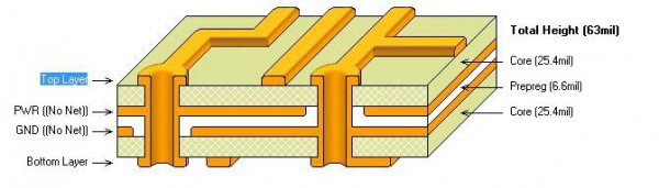
1) Lamination
A new raw material called semi curing sheet is needed here, which is the adhesive between core board and core board (PCB layer number > 4), as well as between core board and outer copper foil, and also plays the role of insulation. The lower layer of copper foil and two layers of semi-cured sheet have been fixed in advance through the alignment hole and the lower layer of iron plate, and then the core plate made is put into the alignment hole. Finally, two layers of semi-cured sheet, one layer of copper foil and one layer of pressure bearing aluminum plate are successively covered on the core plate. The PCB boards clamped by the iron plate are placed on the bracket, and then sent to the vacuum hot press for lamination. The high temperature in the vacuum hot press can melt the epoxy resin in the semi curing sheet, and fix the core plates and copper foils together under pressure. After lamination, remove the upper iron plate of the pressed PCB. Then take away the pressure bearing aluminum plate, which also plays the responsibility of isolating different PCBs and ensuring the smoothness of the outer copper foil of PCB. At this time, both sides of the PCB will be covered with a layer of smooth copper foil. In the future, we will package the printed components (as well as soldered components) on the surface to facilitate the operation of the printed components. Generally, the screen printing layer is placed on the top layer. However, for the main board of electronic products with high failure rate and frequent maintenance, such as TV, computer display and printer, the screen printing layer can be set in the component surface and solder surface.
2) Drilling
In order to connect the four layers of copper foil in the PCB without any contact, first drill through holes to open the PCB, and then metallize the hole wall to conduct electricity. Use the X-ray drilling machine to locate the inner core plate, the machine will automatically find and locate the hole position on the core plate, and then punch a positioning hole for the PCB to ensure that the next drilling is from the center of the hole position. Place a layer of aluminum plate on the punch machine, and then place the PCB on it. In order to improve efficiency, according to the number of layers of PCB, 1-3 identical PCB boards will be stacked together for perforation. Finally, a layer of aluminum plate is covered on the top PCB. The upper and lower layers of aluminum plate are used to prevent the copper foil on the PCB from tearing when the drill bit is drilling in and out. In the previous lamination process, the melted epoxy resin was extruded outside the PCB, so it needs to be cut off. Profiling milling machine cuts the periphery of PCB according to the correct XY coordinate.
3) Copper chemical precipitation on pore wall
Since almost all PCB designs use holes to connect different layers of circuits, a good connection requires a 25 micron copper film on the hole wall. This thickness of copper film needs to be electroplated, but the pore wall is composed of non-conductive epoxy resin and fiberglass board. Therefore, the first step is to deposit a layer of conductive material on the hole wall, and form a 1-micron copper film on the whole PCB surface, including the hole wall, by chemical deposition. The whole process, such as chemical treatment and cleaning, is controlled by the machine.
4) Fix PCB, clean PCB, transport PCB
5) Outer PCB layout transfer
Next, the outer PCB layout will be transferred to the copper foil. The process is similar to the previous inner core PCB layout transfer principle, which is to use the photocopied film and photosensitive film to transfer the PCB layout to the copper foil. The only difference is that the positive film will be used as the plate. The inner PCB layout transfer use the subtraction method and uses the negative film as the board. The circuit is covered by the solidified photosensitive film on the PCB. After cleaning the uncured photosensitive film and etching the exposed copper foil, the PCB layout circuit is protected by the solidified photosensitive film and left behind. The layout transfer of outer PCB use the normal method, and the positive plate is used as the board. The non circuit area is covered by the cured photosensitive film on the PCB. Clean the uncured photosensitive film and electroplate it. Where there is a film, it cannot be electroplated, but where there is no film, it is plated with copper first and then tin. After the film is removed, alkaline etching is carried out, and then tin is removed. The circuit pattern is left on the board because it is protected by tin.
6) Outer PCB etching
Next, a complete automatic pipeline completes the etching process. Firstly, clean the cured photosensitive film on PCB. Then clean the unnecessary copper foil covered by it with strong alkali. Then the tin coating on the copper foil of PCB layout is removed with the tin stripping solution. After cleaning, the layout of 4-layer PCB is completed.
7) Testing
PCB testing is a way to find problems in time, and also a necessary means to prevent more defective products and reduce losses. General inspection includes browning peel strength test and slicing test, patch solder / resistance test.