The quality of solder paste welding is determined by the pressure, precision and reflow soldering furnace of the printing machine, and the mechanical precision and optical identification of the mounter determine the quality of the mounter. Therefore, to improve the quality, we need to regularly calibrate these high-precision machines, at least when there is a problem, we need to think about this. In terms of efficiency, the most important thing is the mounter. One is the speed of the mounter itself, but how to optimize the mounter program. Especially for the final universal machine, it is better to optimize it manually. The other thing that decides the whole process but the production unit can't do is the quality of PCB, including the precision of pad and mark and the design of circuit, which have an impact on the whole patch section.

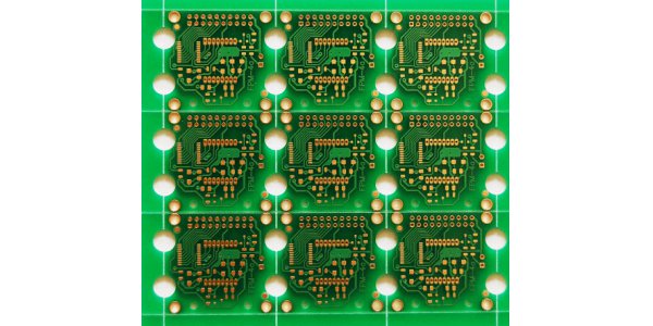
1) Mark point is round or square, with a diameter of 1.0 mm, which can be determined according to SMT equipment. The copper area from mark point to the surrounding area shall be more than 2.0 mm, and mark point shall not be creased, dirty, exposed copper, etc;
2) There must be mark points on the four corners of each large plate or two mark points on the opposite corners, and the distance between the mark points and the edge must be greater than 5 mm;
3) Each small board must have two Mark points;
4) According to the specific equipment and efficiency evaluation, it is not allowed to mark "X" in the FPC panel. 5) when patching, the key areas shall be glued firmly with wide adhesive paper, and then the film shall be checked. If the patching is not smooth, the film shall be pressurized again and checked again;
6) The pad spacing of 0402 element is 0.4 mm; the pad spacing of 0603 and 0805 element is 0.6 mm; the pad is better to be square;
7) In order to avoid undercutting in small area of FPC plate due to undercutting, undercutting is carried out from the bottom;
8) After FPC board is made, it must be vacuum packed after baking; before SMT is put on line, it is better to pre bake;
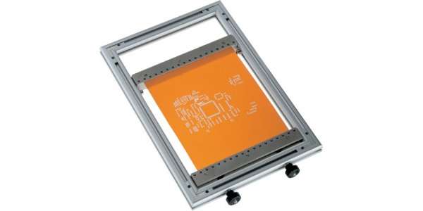
9) The best panel size is within 200mmx150 mm;
10) Four SMT fixture positioning holes with an aperture of 2.0mm shall be reserved at the edge of the panel;
11) The minimum distance between panel edge components and panel edge is 10 mm;
12) As far as possible, each panel should be distributed in the same direction;
13) The gold finger area of each small plate (i.e. hot pressing end and weldable end) is assembled into one piece to avoid 14) the minimum distance between chip element pads is 0.5 mm.

It is estimated that both engineering designers and technologists have experienced such experiences: after FPC production is completed, components need to be welded by SMT; the problem is that as an excellent designer, only knowing some special requirements of SMT process in advance can he maintain high quality and efficiency in SMT production process. Because FPC requires a high flatness of the board itself in the SMT process; in addition, the spacing, mark point setting, panel size and so on will affect the quality and efficiency of SMT. Therefore, as a design engineer of FPC manufacturer, he should know more about some special requirements of SMT and consider the design comprehensively before manufacturing in combination with the FPC process capability. He must be careful not to lose one or lose the other, otherwise he will have endless troubles.
