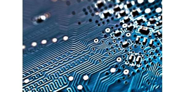
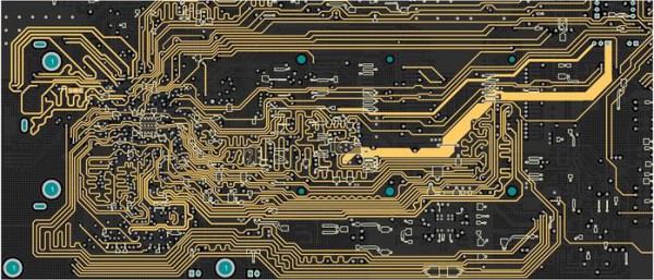
The design of printed circuit board is based on the circuit schematic diagram to realize the functions required by the circuit designer. Printed circuit board design mainly refers to layout design, which needs to consider the layout of external connections, optimized layout of internal electronic components, optimal layout of metal wires and through holes, electromagnetic protection, heat dissipation and other factors. Excellent layout design can save production cost and achieve good circuit performance and heat dissipation performance. Simple layout design can be realized by hand, while complex layout design needs to be realized by computer aided design (CAD). If you want to know the detailed multi-layers printed circuit board manufacturing process, check it out on AiPCBA.

In the design of PCB, following attentions should be paid to avoid arranging important signal lines at the edge of PCB, such as clock and reset signal. The space between the cabinet ground wire and the signal line shall be at least 4 mm, and the length width ratio of the cabinet ground wire shall be kept less than 5:1 to reduce the inductance effect. The device and line that has been located will be locked by the lock function, so that it will not be moved in the future. The minimum width of conductor should not be less than 0.2mm (8mil). In high-density and high-precision printed circuit, the wire width and spacing can generally be 12ml. The principle of 10-10 and 12-12 can be applied to the wiring between IC pins of dip package, that is, when two wires pass between two pins, the pad diameter can be set as 50mil, the line width and wire spacing are 10mil. When only one wire is passed between the two pins, the pad diameter can be set as 64mil, and the line width and wire spacing are both 12mil. When the diameter of the pad is 1.5mm, in order to increase the anti stripping strength of the pad, the pad with length no less than 1.5mm, width of 1.5mm and oblong pad can be used. When the wiring of the pad connection is thin, the connection between the pad and the wiring should be designed as water drop, so that the pad is not easy to peel and the wiring and pad are not easy to be disconnected. In the design of large area copper coating, there should be a window and a cooling hole on the copper coating, and the open window should be designed as a mesh. As far as possible to shorten the connection between high-frequency components, reduce their distribution parameters and mutual electromagnetic interference. Components susceptible to interference shall not be too close to each other, and input and output components shall be kept away from each other as far as possible.

Several special components will be edited in PCB design. First of all, the shorter the connection between the high frequency components, the better. Try to reduce the distribution parameters of the wires and the electromagnetic interference between each other. The easily disturbed components should not be too close. The distance between the components attached to the input and to the output should be as large as possible. Secondly, components with high potential difference: the distance between the components with high potential difference and the connecting line should be increased to avoid damaging the components in case of accidental short circuit. In order to avoid creepage, it is generally required that the distance between copper film wires between 2000V potential difference should be greater than 2mm. If the potential difference is higher, the distance should be increased. Devices with high voltage should be arranged in the place where hands are not easy to reach during debugging. Thirdly, components with too much weight: such components should be fixed with brackets, and for large, heavy and heat generating components, they should not be installed on the circuit board. Fourthly, heating and thermal elements: pay attention to the heating elements should be far away from the thermal elements. More design Rules for PCBA about size Planning and Control of Circuit Board on AiPCBA are available now.
