1、Design steps of Multilayer PCB:
The design process of multilayer PCB is basically the same as that of ordinary PCB. The difference is that the wiring of intermediate signal layer and the division of internal electric layer are needed. In a comprehensive view, the design of multilayer PCB is basically divided into the following steps:
1).The planning of PCB is mainly to plan the physical size of PCB, the package form of components, the installation mode of components, and the structure of board layer, i.e. single-layer board, double-layer board and multilayer board.
2).Working parameter setting mainly refers to working environment parameter setting and working layer parameter setting. The correct and reasonable setting of PCB environment parameters can bring great convenience to the design of PCB and improve the working efficiency.
3).Component layout and adjustment. After the current period of work is accurate, you can import the network table into PCB, or you can directly import the network table by updating PCB in the schematic diagram. Component layout and adjustment is an important work in PCB design, which directly affects the following operations such as wiring and internal layer segmentation.
4).The definition and setting of PCB middle layer. This operation focuses on setting the specific layer structure in the software layer stack manager, mainly setting the number of middle signal layer and internal electric layer, upper and lower structure, etc.
5).Internal power layer segmentation, usually the internal power layer, often more than one power network, often needs to divide the internal power layer into several isolated areas, and connect each area to a specific power network, which is the biggest difference between multilayer board and ordinary board, and also an important link in the design of multilayer circuit board. The structure of the internal layer often directly affects the routing of the power and ground grids, as well as the layout and routing of the components.
6).The setting of wiring rules is mainly to set various specifications of circuit wiring, such as wire width, parallel line spacing, safe spacing between wire and pad, and via size. No matter what wiring method is adopted, wiring rules are an essential step. Good wiring rules can ensure the safety of circuit board wiring, meet the requirements of manufacturing process, and save costs.
7).Wiring and adjustment, the system provides automatic wiring, but often can not meet the requirements of the designer. In practical application, the designer often relies on manual wiring, or part of the automatic wiring combined with manual interactive wiring to complete the wiring work. In particular, the layout and wiring as well as PCB circuit board have the characteristics of internal electric layer. Although the layout and wiring have the sequence, in the design engineering, the layout of circuit board is often adjusted according to the needs of wiring and internal electric layer division, or the wiring is adjusted according to the layout, which is a process of mutual consideration and adjustment.
8).Other auxiliary operations, such as copper laying and teardrop mending, as well as document processing such as report output and save printing, can be used to check and modify PCB circuit board, and can also be used as a list of purchased components.
2、Notes on the design of Multilayer PCB:
In the design of high-speed multilayer PCB, special attention should be paid to the design of layers, that is, how to divide the signal line, power line, ground line and control line in each layer. The general principle is that the analog signal and the analog signal ground should at least guarantee a separate layer. A separate layer is also recommended for the power supply.
3、General principles of Multilayer PCB layer layout:
1) Under the device surface (the second layer) is the ground plane, providing device shielding layer and reference plane for device surface wiring;
2) All signal layers shall be adjacent to the ground plane as much as possible;
3) Try to avoid two signal layers directly adjacent;
4) The main power supply shall be adjacent to it as far as possible;
5) In principle, symmetrical structure design should be adopted. The meaning of symmetry includes: thickness and type of dielectric layer, thickness of copper foil and figure;
6) Symmetry of distribution type (large copper foil layer, line layer).
4、Advantages of Multilayer PCB:
High assembly density, small volume and light weight. Due to high assembly density, the wiring between components (including components) is reduced, so the reliability is improved; the number of wiring layers can be increased, so the design flexibility is increased; the circuit with certain impedance can be formed; the high-speed transmission circuit can be formed; It can be equipped with circuit, magnetic circuit shielding layer and metal core heat dissipation layer to meet the needs of shielding, heat dissipation and other special functions; the installation is simple and the reliability is high
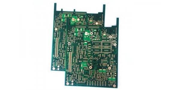
5、Introduction to Multilayer PCB:
The double panel is a medium layer in the middle, and both sides are wiring layers. A multilayer board is a multilayer wiring layer. Between each two layers is a medium layer, which can be very thin. The multilayer circuit board has at least three conductive layers, two of which are on the outer surface, and the remaining one is synthesized in the insulating board. The electrical connection between them is usually realized by plated through holes on the cross section of the circuit board.
PCB manufacturing process is a more complex process. In every production link, corresponding equipment is needed to process, which requires a lot of energy and cost.
6、In the PCB production process, the following production equipment is required:
1) . Engineering production - photo machine, film exposure machine
2). Cutting - oven for cutting machine and baking board
3). Lamination browning production line, laminating machine, plate grinder
4). Drilling - CNC drilling machine
5). Plate grinding machine
6). Metallized hole (PTH) - chemical copper production line (sunk copper wire)
7). Pattern transfer - applicator, UV exposure or LDI
8). Graphic electroplating -- electroplating production line
9). Dry (wet) film fading production line
10). Graphic etching - etching production line
11). Solder mask making - screen printing, UV exposure or LDI
12). Curing oven, tunnel oven
13). Surface treatment -- OSP production line or chemical nickel gold line, chemical nickel palladium gold line
14). Forming - stamping machine or CNC gong machine, cutting machine
15).Test - electric tester, AOI, 3daoi