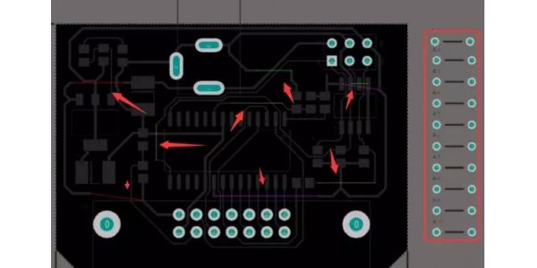
The correct structural design of printed circuit board component layout and wiring is a key factor that determines whether electronic works can work reliably. This article details the printed circuit board component layout and wiring principles.

1. Component layout principles
In the layout design of the printed circuit board, the layout of the components is very important. It determines the degree of neatness and beauty of the board surface and the length and number of printed wires. It also has a certain impact on the reliability of the machine. The following principles should be followed when laying components:1.1 Under normal circumstances, all components should be arranged on one side of the printed circuit board. For single-sided printed circuit boards, components can only be installed on the side without printed circuits; for double-sided printed circuit boards, components should also be installed on one side of printed circuit boards; if insulation is required, There is a 1 ~ 2mm gap between the pad and printed circuit board and the printed circuit board. Where conditions permit, components should be distributed evenly and densely throughout the board.
1.2 On the premise of ensuring electrical performance, components should be arranged parallel or vertical to each other in order to be neat and beautiful.
1.3 Heavy and large components should be placed as close to the fixed end of the printed circuit board as possible, and the center of gravity should be lowered to improve mechanical strength and resistance to vibration and shock, and reduce the load and deformation of the printed circuit board.
1.4 The heat-generating components should be arranged in a position favorable for heat dissipation. If necessary, a heat sink can be installed separately to reduce and reduce the impact on neighboring components. Keep heat sensitive components away from high temperature areas.
1.5 Components that are more sensitive to electromagnetic induction and components with stronger electromagnetic radiation should avoid mutual influence when they are laid out.
2. Wiring Principles for Printed Conductors
After the component layout is completed, you can arrange and draw the connection lines of each component according to the circuit schematic diagram, that is, the wiring design of the printed wire. The wiring has a great impact on the electrical performance of the whole machine, and its principles are as follows:2.1 The common ground wire is generally arranged at the extreme edge of the printed circuit board, which is convenient for the printed circuit board to be installed on the rack and also connected to the rack ground. Low-frequency DC wires and components such as power supplies and filters are arranged on the edge. High-frequency components and wires are arranged in the middle of the printed circuit board to reduce their distributed capacitance to the ground and the case.
2.2 There should be a certain distance (not less than the thickness of the board) between the printed wire and the edge of the printed circuit board. This not only facilitates the installation of rails and machining, but also improves the insulation performance.
2.3 Some printed conductors of a single-sided printed circuit board sometimes have to go around or parallel, so that the printed conductors are relatively long, which not only increases the lead inductance, but also increases the parasitic coupling between the printed conductors. This does not have a significant effect on low-frequency circuits, but it has a significant effect on high-frequency circuits. Therefore, it is necessary to ensure that high-frequency wires, lead wires of the electrodes of transistors, input and output wires are short and straight, and avoid parallel to each other. If individual printed wires cannot go around, in order to avoid the wires crossing at this time, you can use cross wires. For high-frequency circuits, avoid using external wires to cross. If there are many crossed wires, it is best to use a double-sided printed circuit board and print the wires on both sides of the board to make the wires short and straight. When using a double-sided board, the printed wires on both sides should be avoided to be parallel to each other to reduce the parasitic coupling between the wires.
3. What to do when wires cross
3.1 Handle the power and ground wires well, effectively suppress the interference caused by the common impedance, and achieve the effect of doing more with less.3.2 The layout of printed conductors should be neat, beautiful, organized, and the wiring and component layout should be coordinated. Under the premise of electrical performance, the wiring should be parallel to the same direction, and the 45-degree angle should be used at the turning point of the printed conductor to avoid the use of acute and right angles.
