Detailed Introduction of Different Types of PCB Layers
Posted: May 14, 2022
By: Bonnie
1. Signal Layers
The signal layer is used to complete the wiring layer of the copper foil traces of the printed circuit board. The signal layers include Top Layer, Bottom Layer, Mid Layer 1 ... 30. These layers are all layers with electrical connections, which is the actual copper layer. The middle layer refers to an intermediate board layer used for wiring, and in this layer are conductive wires.When designing a double-sided board, generally only Top and Bottom are used. When the number of printed circuit board layers exceeds 4 layers, Mid is required.
Protel provides 16 signal layers.

2. Internal Planes
This type of layer is only used for multi-layer boards. These layers are generally connected to the ground and the power supply, and become the power supply layer and the ground layer. They also have the function of electrical connection and are also actual copper layers. The entire copper film.We call double-layer boards, four-layer boards, and six-layer boards, and generally refer to the number of signal layers and internal power / ground layers.
Protel provides 16 internal power / ground planes.
3. Mechanical Layers
Used to set the overall dimensions, data marks, alignment marks, assembly instructions and other mechanical information of the circuit board. This information varies depending on the requirements of the design company or PCB manufacturer.Designing a double sided board requires only the default option Mechanical Layer 1. There are Mech1-Mech4 (4 mechanical layers).
Execute the menu command Design | Mechanical Layer to set more mechanical layers for the board. In addition, the mechanical layer can be attached to other layers and output and displayed together.
Protel can select up to 16 mechanical layers.
4. Solder Mask
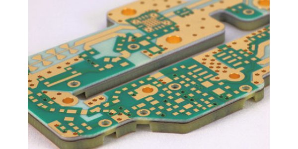
Apply a layer of paint, such as a solder mask, to areas other than the pads to prevent tin from being applied to these areas. The solder mask is used to match the pads during the design process and is automatically generated.Including the Top solder and the Bottom solder, its role is opposite to the solder paste layer, refers to the layer to be covered with green solder. This layer is non-stick soldering, preventing excess soldering of adjacent soldering points during short circuiting. The solder resist layer covers the copper film wire, and the protective area around the pads and vias on the printed circuit board is drawn on the solder resist layer.
The anti-copper film oxidizes in the air too quickly, but leaves a place at the solder joint and does not cover the solder joint.
5. Paste Mask
Including the Top paste and Bottom paste, refers to the surface mount pads we can see exposed, that is, the part that needs to be coated with solder paste before soldering. Therefore, this layer is also useful for hot air leveling of pads and welding stencils.It functions similarly to a solder mask, except that the pads of the corresponding surface-mount components are soldered during machine soldering. If the board is full of Dip (through-hole) components, this layer does not need to output Gerber files. Before putting the SMD components on the PCB, you must first apply solder paste to each SMD pad. The Paste Mask file must be used on the stencil for tinning, and the film can be processed.
The most important point of the Gerber output of the Paste Mask layer is that this layer is mainly for SMD components. At the same time, compare this layer with the Solder Mask introduced above to clarify the different roles of the two. The film pictures are very similar.
6. Keep Out Layer
Defines areas on the board where components and routing can be effectively placed. Draw a closed area on this layer as the effective area for routing. Outside this area, you cannot automatically place and route.In the subsequent wiring process, wiring with electrical characteristics must not exceed the boundary of the prohibited wiring layer.
It is used for automatic wiring, and manual wiring is not required.
7. Silkscreen Overlay
The silk screen layer is used to draw text descriptions and graphic descriptions, such as component names, component symbols, component pins and copyrights, etc., to facilitate future circuit soldering and troubleshooting.Including the Top overlay and the Bottom overlay. Generally, the various label characters are on the top screen printing layer, and the bottom screen printing layer can be closed.
8. Multi Layer
The pads and penetrating vias on the circuit board need to penetrate the entire circuit board and establish an electrical connection relationship with different conductive pattern layers. Therefore, the system specifically sets an abstract multi-layer.
Generally, the pads and vias must be set on multiple layers. If this layer is closed, the pads and vias cannot be displayed.
9. Drill Layer
Used to draw the drilling hole diameter and hole positioning (such as pads, vias need to be drilled).There are 2 layers: Drilling Drawing, Guiding Layer
10. Other layers
"Connect", "DRC Error", 2 of "Visible Grid", "Pad Holes" and "Via Holes". Some of these layers are used by the system itself, such as the visual grid layer, which is designed to facilitate the positioning of the designer when drawing.For hand-drawn double-sided printed circuit boards, the most commonly used are Top Layers, Bottom Layers, and Top Silkscreen. Each layer can choose a color they are accustomed to, generally red for the top layer, blue for the bottom layer, green or white for text and symbols, and yellow for pads and vias.
More resources:
Do you have any questions about the above-mentioned? Contact us now, we will reply to you soon.
Is the article useful to you?
No
Yes(
9
)
9
567
3
Share to:
