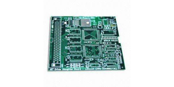
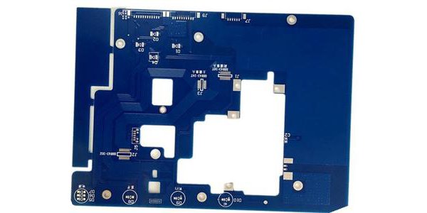
There are many kinds of PCB surface treatment, PCB proofing personnel should choose according to the performance and requirements of the board.
Hot air solder leveling (HASL) is an advanced technology developed in the 1980s. In the middle and late 1990s, it occupies more than 90% of the total PCB surface coating (plating). Only in the late 1990s, due to the in-depth development of Surface Mount Technology (SMT), the share of Hal in PCB gradually decreased. However, at present, the share of Hal in PCB surface coating (plating) is still about 50%. Although the high density development of SMT will reduce the application probability of Hal in PCB, the application of Hal technology in PCB production still has a long life force. Even if lead solder (lead-free green solder) is prohibited, lead-free Hal technology and process will be developed and applied.
Usually we will call it tin spraying, which is commonly used in the early PCB processing. Now it is divided into lead-free tin spraying and lead-free tin spraying. After PCB is finished, the copper surface can be completely wetted (completely covered with tin before welding). It is suitable for lead-free welding, mature process, low cost and suitable for visual inspection and electrical measurement. However, tin spraying is not suitable for wire binding. Due to the problem of surface flatness, it is also limited in SMT; it is not suitable for contact switch design. Copper dissolves when tin is sprayed, and the board is subjected to a high temperature. It is not convenient to spray tin on special thick or thin plates.

The tin / lead alloy layer of Hal has also encountered problems and challenges in the application of SMT, mainly due to the large surface tension of molten tin / lead alloy (about 6 ∽ 8 times of that of water), the formation of inter-metallic compound (IMC) at high temperature and the high temperature (230 - 250 ℃) thermal shock on PCB during Hal process.
<1> The problems and challenges brought about by too high surface tension of molten Sn / Pb alloys are discussed. With the development of PCB for surface mounting to high density, the density of PCB connecting pad (PAD) is increasing, and its size is getting smaller and smaller. Under the condition of coating the same thickness of molten tin / lead alloy, due to the effect of surface tension, the tin / lead alloy layer on the small size connecting plate presents "turtle back" phenomenon. The "turtle back" phenomenon will become more and more serious with the development of high density (or miniaturization of connection plate). As a result, the "point" contact between the pins of components (especially SMD surface mounted devices) and the connecting plate will be formed, which will affect the reliability of welding (especially displacement and dislocation in high density welding).
<2> The effect of the formation of tin / copper alloy compounds at high temperature. If the tin / lead alloy layer is thinned by increasing the hot air velocity (hot air pressure) of Hal to eliminate the "turtle back" phenomenon and obtain the flatness on the connecting plate, it also brings about welding reliability problems. At high temperature, a variety of tin / copper alloy compounds, such as Cu3Sn, Cu3Sn2, Cu4Sn3... Cu6Sn5, Cu2Sn3, will be formed between the interface of tin and copper, the type and thickness of various alloy compounds formed are related to the thickness of tin / lead alloy in Hal, the times of Hal and the holding time at high temperature. At the same time, it is also related to the number of high temperature welding. For example, the higher the treatment temperature of Hal, the longer the time and the more times of welding at high temperature, etc., all of these will increase and thicken the non weldable copper / tin alloy compounds (such as Cu3Sn, Cu3Sn2). When the thickness of Sn / Pb alloy layer is very thin (eg. thickness ≤ 2um), it is possible to form all non solderable copper / tin alloy compounds. This kind of compound between copper and tin with very thin thickness seems to have good planarity, but it is not solderable or the welding is not firm (false welding), thus affecting the welding reliability. There are many examples and lessons in this respect
<3>Thermal shock of hot air leveling to PCB. PCB is impacted by high temperature (230 - 250 ℃ / 3 ∽ 5sec) during hot air leveling, which will affect the service life of PCB. Some people have done experiments and statistics. The effect of hot air leveling on the service life of PCB is mainly manifested in the porosity failure rate of PCB (especially for multilayer boards). The porosity failure rate of conventional multilayer boards after hot air leveling is about 50% higher than that without hot air leveling (for example, the porosity failure rate of multilayer boards with conventional FR-4 materials after hot air leveling will increase by 1 * 10-9 To 2 * 10-9), which indicates that the effect of CTE (thermal expansion coefficient) in Z direction of PCB on hole metallization is the main one. For the multilayer board with buried / blind hole structure, the effect of hot air leveling on the porosity failure rate is much smaller. At the same time, it should be understood that the hot air leveling process will also affect other PCB properties (such as warpage, internal stress, interlayer bonding force, etc.).

2) OSP (organic protective film)
In the early days, OSP organic solder-ability preservatives was called pre flux. In fact, it is a kind of ABI alkyl benzimidazole compounds with high heat resistance, and its decomposition temperature is generally required to be above 300 ℃. Therefore, it can well protect the fresh copper surface from oxidation and pollution. In high temperature welding, due to the role of solder to remove OSP, the fresh copper surface is exposed and quickly and firmly welded with the solder.
OSP process is simple, the surface is very flat, suitable for lead-free soldering and SMT. OSP is easy to rework, easy to operate, suitable for horizontal line operation. OSP board is suitable for multiple processing (such as: OSP + ENIG), low cost and environment-friendly. However, OSP has the limitation of reflow soldering times (the film will be damaged if the welding is thick for many times, and basically there is no problem for twice welding), so it is not suitable for crimping technology and wire binding. The visual inspection and electrical measurement are not convenient. N2 gas protection is required for SMT. SMT rework is not suitable and the storage condition is high. The disadvantage of OSP film is that the protective film is very thin, easy to scratch (or scratch), so it must be carefully operated and operated. At the same time, after many times of high temperature welding process, the OSP film (refers to the OSP film on the non welded connecting plate) will change color or crack, which will affect the solder-ability and reliability. However, it is ideal for high density welding with less welding times (such as 1-2 times). It is OSP film that has these advantages, so its application in PCB is expanding. At present, the application of OSP film in PCB surface coating (plating) has accounted for about 30%. In the past two or three years and in the future, due to the continuous improvement of OSP composition, the heat resistance temperature and heat resistance of OSP will continue to increase. Therefore, the application ratio of OSP film in PCB will be further expanded.
