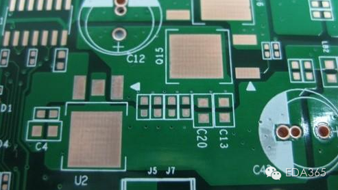
OSP
OSP stands for Organic Solderability Preservatives (Anti-oxidation), also known as copper shielding agent.
Its essence is to act as a barrier between copper and air. The process is as follows: on the surface of bare copper, a layer of organic skin film is grown by chemical method, which has anti-oxidation, heat shock resistance and moisture resistance to protect the copper surface from rusting, oxidation and sulfuration in normal environment.
However, in the subsequent high temperature welding, the protective film must be easily removed by flux, so that the copper surface can be combined with molten tin to form a solid solder joint in a very short time.
The technological process of OSP is degreasing, secondary water washing, micro-erosion, secondary water washing, acid washing, DI water washing, film-forming air drying, DI water washing, drying.

1. Degreasing
The effect of oil removal directly affects the quality of film formation. Poor oil removal results in uneven film thickness. On the one hand, the concentration can be controlled within the technological range by analyzing the solution. On the other hand, it is necessary to check whether the degreasing effect is good or not. If the degreasing effect is not good, the degreasing fluid should be replaced in time.
2. Microerosion The purpose of Micro-etching is to form rough copper surface and to facilitate film formation. The thickness of Micro-etching directly affects the film forming rate, so it is very important to form a stable film thickness and maintain the stability of Micro-etching thickness. Generally, it is appropriate to control the thickness of Micro-etching at 1.0-1.5um. Before each shift production, the micro-corrosion rate can be measured, and the micro-corrosion time can be determined according to the micro-corrosion rate.
3. Filming It is better to use DI water for washing before film forming in order to prevent fouling of film forming liquid. DI water is also the best water for washing after film formation, and the PH value should be controlled between 4.0 and 7.0 in order to prevent the film from being polluted and destroyed. The key of OSP process is to control the thickness of anti-oxidation film. The film is too thin and has poor heat shock resistance. During over-reflow welding, the film can not withstand high temperature (190-200 degrees C), which ultimately affects the welding performance. On the electronic assembly line, the film can not be well dissolved by flux and affects the welding performance. It is suitable to control the film thickness between 0.2 and 0.5 um.
OSP PCB Complete Manufacturing Guide
OSP is the abbreviation of Organic Solder-ability Preservatives. Simply put, OSP is to grow a layer of organic film on a clean bare copper surface by chemical methods. This layer of film has anti-oxidation, thermal shock, and moisture resistance to protect the copper surface from continuing in the normal environment. Rusting (oxidation or vulcanization, etc.); however, in the subsequent high-temperature soldering, this protective film must be easily removed by the flux, so that the exposed clean copper surface can be melted with the molten solder in a very short time Immediately combine to become a solid solder joint.
OSP manufacturing flow:
Degreasing-->Secondary Water Washing-->Micro Erosion-->Secondary Water Washing-->Acid Washing-->DI Water Washing-->Film-forming Air Drying-->DI Water Washing—>Drying
