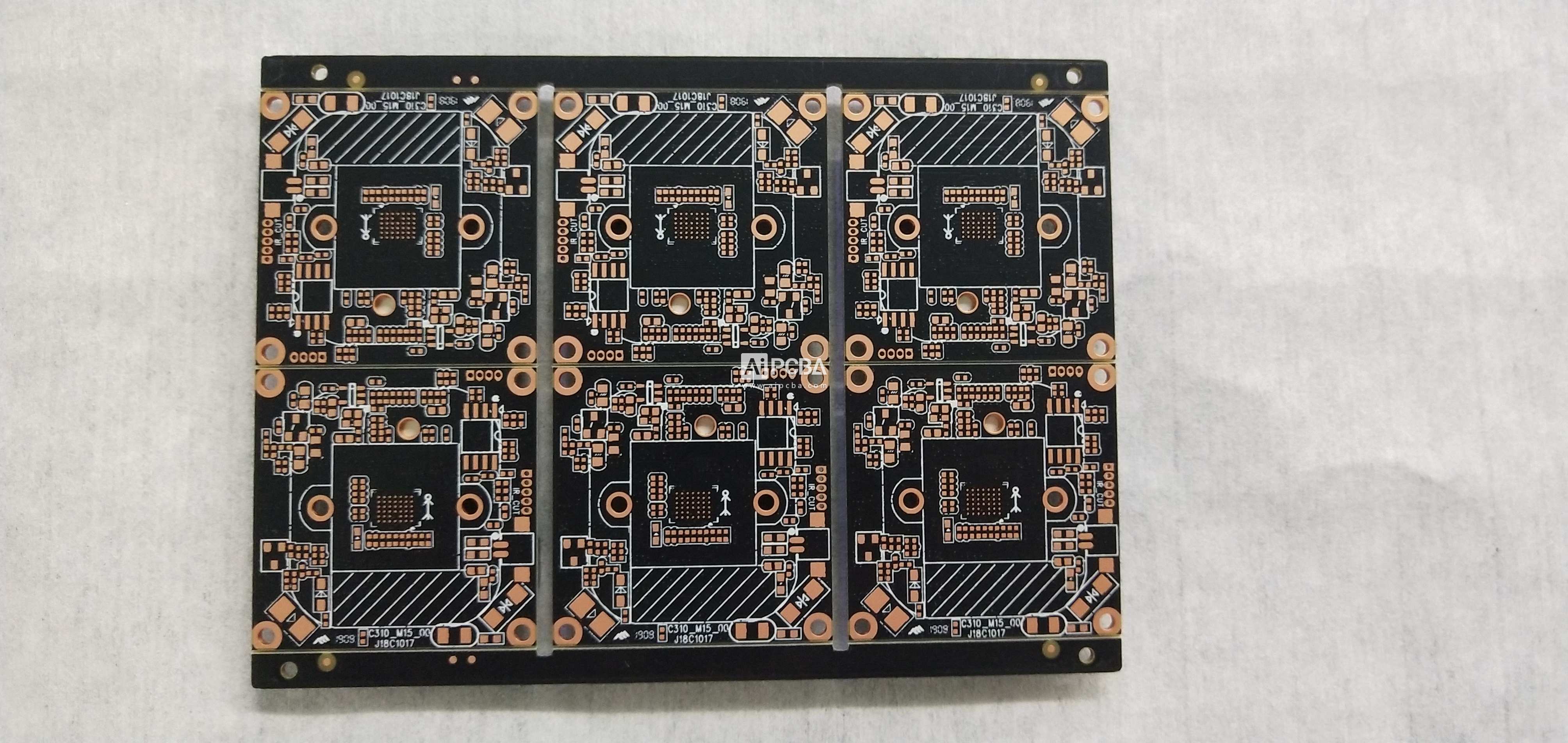
High Density Interconnection printed circuit boards (HDI PCBs) use the latest technology to increase the use of PCBs in the same or smaller area. This has driven major advances in mobile phones and computer products, also it's generating revolutionary new products. This includes touch-screen computers and 4G communications and military applications, such as avionics and intelligent military equipment.
High density interconnection (HDI) printed circuit boards are characterized by high density properties, including laser microporous, thin wires and high performance thin materials. This increased density can support more functions per unit area. High-tech high-density interconnection (HDI) printed circuit boards contain multi-layer stacked copper-filled microholes (high-order HDI printed circuit boards), which can be used to create more complex interconnections. These very complex structures provide the necessary wiring solutions for today's large pin-to-pin chips used in mobile devices and other high-tech products.

High Density Interconnection (HDI) Architecture:
1 + N + 1 - PCB includes a high density interconnection layer.
i + N + i (i ≥2) - PCB includes two or more high density interconnection layers. Microholes in different layers can be staggered or stacked. Multilayer stacked copper microporous filling is common in challenging design.
Arbitrary High Density Interconnection Board (HDI) - All layers of PCB are high density interconnection layers. Conductors on any layer of PCB can freely connect with each other through multi-layer stacked copper microporous structure ("arbitrary layer conductive hole"). This provides a reliable interconnection solution for highly complex large pin-number components, such as CPU and GPU chips on handheld and mobile devices.
Advanced Ability: Micropore
Microholes are formed by laser drilling, usually with diameters of 0.006"(150 m), 0.005"(125 m) or 0.004"(100 m). They are optically aligned with the corresponding pad diameters of 0.012"(300 m), 0.010"(250 m) or 0.008"(200 m), so more wiring density can be obtained. Microvoids can be directly designed on or off the pad. They can be staggered or stacked with each other. They can be filled with non-conductive resins and plated on the surface of copper cap or directly. Micropore design is valuable when wiring for fine pitch BGA, such as 0.8 mm pitch and below.
In addition, when wiring 0.5 mm pitch components, interleaved micro-porous structures can be used; however, when wiring micro-BGA (such as 0.4 mm, 0.3 mm or 0.25 mm pitch components), stacked micro-porous (SMV ®) is required to be accomplished by inverted pyramid wiring technology.
Schindler has many years of production experience in high density interconnection (HDI) products, and is the pioneer of the second generation of micropore or stacked micropore (SMV ®). SMV technology provides solid copper stacked microholes to support micro BGA wiring solutions.
Schindler has completed the development and can provide all types of microporous technology solutions for your next generation of products.
The following table shows Schindler's complete microporous technology.
Standard or first generation micropore
Create wiring density (eliminate through holes)
Reduce the number of layers
Strengthen electrical characteristics
Standard micropore is limited to layer 1 - 2 and 1 - 3
Stacked micropore (SMV®) or second generation micropore
Allow increased wiring density on multiple layers
Provide wiring solutions for next generation applications
1 mm - 0.8 mm - 0.65 mm - 0.5 mm - 0.4 mm - 0.3 mm and 0.25 mm
Providing filling copper microvoids to eliminate potential welding voids
Provide heat dissipation management solutions
Improving current carrying capacity
Provide flat welding surface for BGA
Technology of Allowing Arbitrary Layer Interconnection
Deep micropore (DpMV™)
It can be used in more dielectric materials or in minimal size graphics design.
Improving impedance performance
Provide RF micropore solutions
Provide filled copper
Improving Current Bearing Capacity and Heat Dissipation Management
Provide flat welding surface for BGA
Deep stacked microvoids (DpSMV™)
Provide more microporous dielectric layers for radio frequency applications
Graphic Design with Minimal Size Retained on Multiple Layers
Improving Signal Integrity
Provide filled copper
Improving Current Bearing Capacity and Heat Dissipation Management
Provide flat welding surface for BGA
Arbitrary Interlayer High Density Interconnection (HDI)
Multilayer stacked copper-filled microporous structure
1.2/1.2 mil line/spacing
4/8 mil Laser Hole/Chassis Size
Material options:
High temperature FR4
Halogen-free
High Speed (Low Loss)

