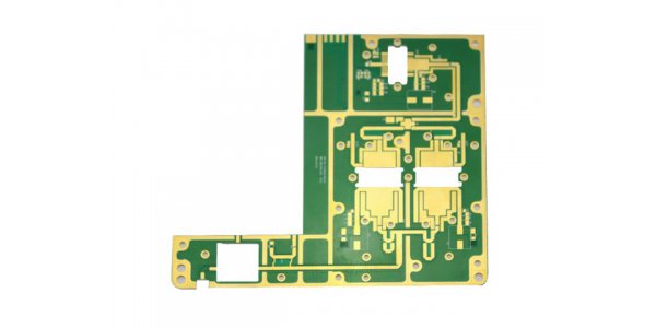
PCB lamination and lamination have many factors to consider, so it is a more complex thing. But we need those key factors to figure out what we want to accomplish. Then we can find a PCB lamination and stacking sequence that meets our requirements. The EMC analysis of multilayer printed circuit board can be based on Kirchhoff law and Faraday law of electromagnetic induction. According to Kirchhoff's law, any time domain signal must have a path with the lowest impedance. We usually refer to I as signal current, I 'as map current, and the layer where I' is located is called map plane layer. If the power layer is below the signal current, the mapping current loop is achieved by capacitive coupling. According to Faraday's law of electromagnetic induction, it can be concluded that the larger A is, the greater E is:

According to the law, the following basic principles should be followed in the layering and stacking of multilayer printed boards
① The power supply plane should be as close as possible to the grounding plane and should be below the grounding plane.
② The wiring layer should be arranged adjacent to the image plane layer.
③ The impedance between power source and formation is the lowest.
④ A stripline is formed in the middle layer and a microstrip line is formed on the surface. They have different characteristics.
⑤ The important signal line should be close to the stratum.
Stacking and layering of PCB
① Laminate
This board can only be used for low speed design. EMC is poor.
② Four layer plate
By the following stacking sequence. The advantages and disadvantages of different layers are described below
|
|
The first floor |
The second floor |
The third layer |
The fourth floor |
|
The first case |
GND | S1+POWER | S2+POWER | GND |
|
The second case |
S1G1 | GND | POWER | S1G2 |
|
The third case |
GND | S1 | S2 | POWER |
In the first case, it should be the best of the four laminates. Because the outer layer is the stratum, it can shield EMI. At the same time, the power layer is very close to the stratum, which makes the internal resistance of the power source smaller and achieves the best effect. But the first case can not be used when the board density is relatively high. Because in this way, the integrity of the first layer cannot be guaranteed, and the signal of the second layer will become worse. In addition, this structure can not be used in the case of high power consumption of the whole board.
The second situation in the table is the most commonly used method. The structure of slave board is not suitable for high speed digital circuit design. Because in this structure, it is not easy to maintain low source impedance. Take a plate 2mm as an example: Z0 = 50ohm. The line width is 8mil. The thickness of copper foil is 35 μ M. In this way, the signal between the first layer and the formation is 0.14mm. The formation and power layer are 1.58mm. This greatly increases the internal resistance of the power supply. In this structure, because the radiation is to the space, it is necessary to add shielding board to reduce EMI.
In the third case in the table, the signal line quality on S1 layer is the best. S2 is the second. It can shield EMI. But the impedance of power supply is large. This board can be used when the power consumption of the whole board is high and the board is an interference source or is close to the interference source.

③ Six layer plate
|
|
The first floor |
The second floor |
The third floor |
The fourth floor |
The fifth floor |
The sixth floor |
| A | S1 | GND | S2 | S3 | POWER | S4 |
| B | S1 | S2 | GND | POWER | S3 | S4 |
| C | S1 | GND | S2 | POWER | GND | S3 |
| D | GND | S1 | POWER | GND | S2 | GND |
A case, is one of the common ways, S1 is a better wiring layer. S2 is the second. But the plane impedance of power supply is poor. Attention should be paid to the influence of S2 on S3 layer.
In case B, S2 layer is a good wiring layer, and S3 layer is better. The plane impedance of the power supply is good.
In case C, this case is the best of the six layer boards. S1, S2 and S3 are all good wiring layers. The plane impedance of the power supply is good. What's more, the wiring layer is one layer less than the first two cases.
In case D, the performance of the six layer board is better than the first three, but the wiring layer is less than the first two. This situation is often used in the backplane.
