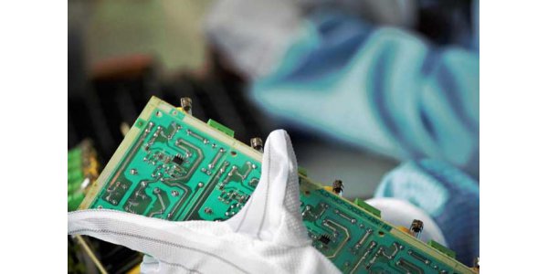
Solder thieves are often heard in the wave soldering process to solve the problem of solder bridges and shorted circuits. When the device process the wave soldering it is often easy to cause the tin connection at the tail end of the device. In order to avoid this defect in production, it is necessary to add a pair of dummy pads at the tail of the device to pull the solder to avoid the phenomenon of tin connection.
The Principle of Solder Thieves
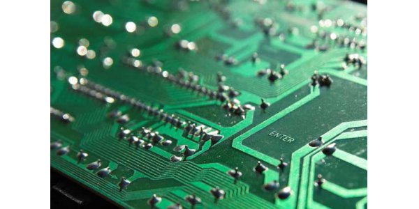
1) The main purpose of the solder thieves setting is to prevent the solder feet of the components on the circuit board soldered by wave soldering from sliding out of the wave soldering surface.The solder bounce buffer area is designed for the tin of the last solder joint to be pulled away from the solder joint after the breakage due to the cohesive rebound of the tin, causing a short circuit with the neighboring solder joints in front of it.
This solder bounce behavior usually occurs in the advective wave of wave soldering and less often in the chip wave.
2) In addition, PIN components and components with the entire row of solder feet parallel to the direction of wave soldering are more prone to short-circuit problems caused by solder rebound.
Whether it is SO (Small Outline) packaged SMD parts or the solder pins of plug-in connectors, as long as they are wave-soldered, there is a chance to form this kind of soldering springback short circuit.
Three Ways to Deal with Solder Thieves in PCB Design
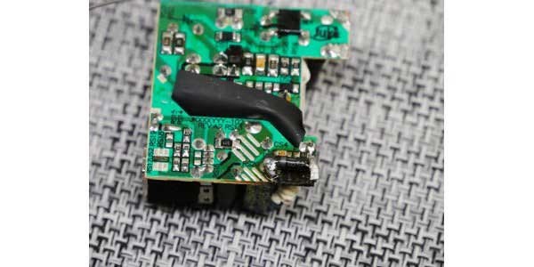
In PCB design, if the components packaged in SOP, QFP, dip, sip, zip series are used, the solder pads need to be stolen. There are three ways to deal with it.
1) Enlarge the pad of side foot
This method is more suitable for the components of the QFP series package. During reflow soldering, the enlarged edge pads can increase the gravitational force of the edges of the components, which is beneficial to the center alignment and positioning of the components.
In wave soldering and manual soldering of PCB, the enlarged edge pads can play a role in solder thieves, which is beneficial to the one-time success rate of soldering. The size requirements of the edge pads are as follows:
a. The length of the pad is the same as that of other pin pads.
b. The width of the pad is 1.5-2 times that of other pin pads.
2) Increase the solder thieves pad
This method is more suitable for SOP series packaged components. The so-called addition of solder thieves pads means that on the basis of the original package, an edge pad is added to achieve the purpose of not soldering the component pins on the PCB. Specific requirements are as follows:
a. When the pitch of the package pins is less than 1.27mm, solder thieves pads must be added.
b. The shape, size and type of the solder thieves pad should be the same as other pin pads.
c. The spacing between the solder thieves pad and the end pad should be equal to the pin spacing of the package.
d. The solder thieves pad on the back should be added in the downstream direction of the PBA direction;
e. The solder thieves pad should be in the same network or floating as its neighboring end pad, and should not conflict with the end pad, so as to avoid shorted circuit of different networks on the PCB when the solder thieves pad and the end pad are welded together.
f. If the solder thieves pad is located inside or covering the silk screen of the outer frame of the component, the silk screen of the outer frame should be adjusted so that the solder thieves pad is located outside the silk screen of the outer frame of the component, so as to avoid welding dislocation.
3) Increase the trailing pad
This method is more suitable for DIP, SIP, ZIP and other series packaged components. The so-called addition of trailing pads means that on the basis of the original PCB package, the back of the end pads in the direction of the PBA is changed to a conical shape, and the tip of the cone is away from the direction of the PBA. Specific requirements are as follows:
a. When When the package is parallel to the direction of the PBA, only the trailing pad is added to the end pin;When the package is parallel to the direction of the PBA, only the trailing pad is added to the end pin;the package pin spacing is less than 2.0mm, a trailing pad must be added.
b. When the package is parallel to the direction of the PBA, only the trailing pad is added to the end pin.
c. When the package is perpendicular to the direction of the PBA, add a trailing pad every other pin.
SMT service in AiPCBA
AiPCBA focuses on a one-stop service for SMT assembly, PCB production, component procurement, assembly, and testing. It is located in Baoan, Shenzhen. The SMT factory covers an area of about 3,500 square meters, as well as various professional testing equipment. At the same time, It has an experienced and professional manufacturing team and customer service team. There are 5 SMT production lines, equipped with new imported placement machines, eight-temperature reflow ovens, automatic solder paste printers, wave soldering, and other high-end equipment, and equipped with AOI, XRAY, SPI, intelligent solder paste detectors, automatic Sub-board machine, BGA rework station, conformal paint spraying and other equipment, focusing on R&D prototyping, small and mass volume SMT assembly, test assembly and other services. The 48-hour sample delivery rate exceeds 95%.
AiPCBA's one-stop PCBA manufacturing service has been widely used in AI artificial intelligence hardware, communication equipment, automotive electronics, industrial control, security, medical, Internet of Things, new energy, rail transit, and other fields; we meet customers with personalized manufacturing and flexible manufacturing Service requirements for hardware PCBA circuit boards from samples, small and medium batches to mass production. Learn more about AiPCBA PCB Assembly service.
AiPCBA's self-developed product online PCBA flexible intelligent manufacturing platform is committed to providing customers with one-stop PCBA prototype production and mass production services. A one-stop PCBA online quotation tool is provided here. You only need to upload your Gerber and BOM files, and AiPCBA can complete all quotations for you within 20 seconds.