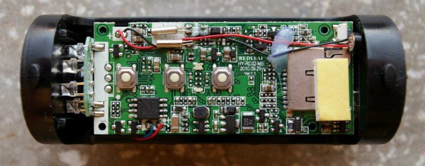
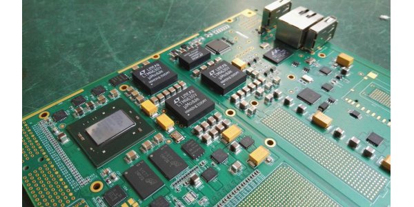
Before welding:
1) Worktable: it must be clean, clean and anti-static, anti-static tools / tools should be used, and anti-static wrist strap should be worn.
2) Tools: there should be tin wire holder, component box, welding gun, welding platform, tweezers, scissors and other welding tools and protective tools.
3) Circuit board: check PCB circuit for short circuit, open circuit, etc.
4)Materials: please confirm the correct components, whether the components have polarity requirements, whether the pads and component feet are oxidized. If so, polish them with fine sandpaper and apply flux before welding.

During welding:
1) Safe and scientific use of electric soldering iron. The soldering iron should be grounded to prevent breakdown of components due to electric leakage during welding. It is recommended to use white adjustable electric iron. The temperature of soldering with lead is about 350 °C and that of lead-free welding is about 380 °C. If there is an oxide layer on the soldering iron head, it is necessary to wipe it off on a high-temperature sponge. Solder the iron before use: when the soldering iron is heated to just melt the solder, apply flux, and then evenly coat the solder on the solder head. Turn off the power supply of soldering iron when it is not in use.
2) Component welding sequence: Based on the principle that the components welded first will not affect the welding of the later components, generally, the components with small volume such as resistance and capacitance are welded first, then the components with larger volume are welded, and the connector is finally welded.
3) Placement of components on the board: the components should be placed in order, in the middle, close to the board surface, and pay attention to the polarity of components.
4) Welding operation posture: the distance between soldering iron and nose should be 20-30cm.
5) Requirements for welding: all components shall not be moved. Do not apply pressure to the welding joint. Firstly, use the solder to contact the solder joint, and then use the soldering iron head to melt the solder along the 45℃ direction. After the solder melts and submerges the component pin, gently lift up along the pin. The welding time is about 2-3 seconds. Do not shake the components before soldering tin is completely solidified, so as to avoid false soldering. Pay attention to properly use flux.
6) The welding time shall not be too long, and repeated welding shall be avoided as far as possible to avoid damaging the components.
After welding:
1) Check whether there is leakage welding, wrong welding (polarity reverse welding), short circuit, false welding and other phenomena.
2) Check whether the solder joint has proper solder. The solder joint should be conical, full, smooth and even, without pinhole, luster, burr, gap and crack. The surface of solder joint should be clean without rosin stain. Solder should surround the pin and should not be too much. If there is a lead, the exposed length of the pin is between 1-2mm.
3) The welding waste should be cleaned up and put into the garbage can in time.
4) Welding tools should be put back in place after use.
5) Use the washing water correctly to clean the residues on PCB, such as tin slag, tin chips, component pins, etc. Protection measures should be taken, because the washing water is volatile and combustible. The leftovers should be packed and placed well, and should not be wasted.
6) Power on test: measure the power input terminal for short circuit with the resistance gear of multimeter, if any, it should be eliminated before power on. Then check the circuit according to the schematic diagram.
7) After power on, the IC must be assembled according to the list before commissioning. After completion, the PCB should be packed with static bag, and cannot be placed at will.

Welding specification for mounting elements:
1) Use tweezers to carefully place the SMD component on the PCB board, align it with the pad, and place it in the center, and the component direction is correct.
2) Before welding, the solder pad should be coated with flux and treated with soldering iron to avoid poor tin plating or oxidation. The components need not be treated.
3) Keep the tip of soldering iron parallel to the pin to be welded to prevent overlap due to excessive solder.
4) When using the soldering iron, the soldering iron can only slide over the pin slightly, otherwise the pin of the SMD component will be bent.
5) After welding all the pins, check the quality of the solder joints: the solder joints should be smooth, full and bright, and there should be no false soldering or missing soldering.
