What is PCB surface finish?
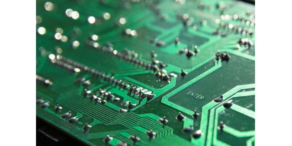
PCB surface finish refers to the process of artificially forming a surface layer with different mechanical, physical and chemical properties of the substrate on the components and electrical connection points of the PCB. If the surface treatment of the circuit board is not carried out, it will be easy to form false welding and virtual welding. In severe cases, the pads and components cannot be welded. The purpose of surface treatment is to ensure good solderability or electrical performance of the PCB.
The most basic purpose of surface treatment is to ensure good solderability or electrical properties.
Because the copper mostly exists in the form of oxides in the air, which seriously affects the solderability and electrical performance of the PCB, the surface treatment of the PCB is required.
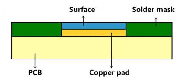
As shown, the surface finish is on the outermost layer of the PCB and on top of the copper, acting as a "coating" of the copper.
The types of surface finish
There are two main types of surface treatments for PCB: metallic and organic.
HASL, ENIG, ENEPIG, Immersion Gold and Immersion Tin belong to metal surface molding, while OSP and carbon ink belong to organic surface finish.
(1) HASL ( hot air solder leveling )
HASL, also known as hot air solder leveling, is a process of coating molten tin-lead solder on the surface of the PCB and leveling it with heated compressed air to form a layer of copper oxidation resistance.
This provides a coating with good solderability.
Solder and copper form a copper-tin intermetallic compound at the junction during hot air leveling. The thickness of the solder to protect the copper surface is about 1-2 mils.
|
HASL advantage |
HASL disadvantage |
|
1. Good solderability during component soldering. 2. Avoid copper corrosion. |
1. HASL surface finish is not acceptable for delicate parts. 2. High thermal stress during the process can cause circuit board defects. |
(2)OSP ( Organic Solderability Preservatives )
OSP surface finish is a common PCB surface treatment technology. It is to chemically grow a layer of 0.2~0.5um organic film on the clean bare copper surface. This film has the ability to resist oxidation, thermal shock and humidity. It is used to protect the copper surface from rusting in the normal environment.
However, in the subsequent high temperature welding, this protective film must be easily removed by the flux, so that the exposed clean copper surface can be immediately combined with the molten solder to form a solid solder joint in a very short time.
|
OSP advantage |
OSP disadvantage |
|
1. The OSP surface is flat and even. 2. OSP film has good thermal shock resistance. 3. Relatively simple process, high yield and low cost. 4. The temperature of the water-soluble operation can be controlled below 80℃, which will not cause the problem of bending and deformation of the substrate. |
1. The formed protective film is extremely thin, and the OSP film is easily scratched (or scratched). 2. After the PCB is soldered at high temperature for many times, the OSP film will be discolored, thinned and oxidized, which will affect the solderability and reliability. |
(3)ENIG ( Immersion Au)
The immersion gold process is not as simple as organic coating, and the immersion gold seems to put a thick armor on the PCB. In addition, the immersion gold process is not like an organic coating as a rust barrier, which can be useful and achieve good electrical properties during long-term use of the PCB. Therefore, the immersion gold is to wrap a thick layer of nickel-gold alloy with good electrical properties on the copper surface, which can protect the PCB for a long time.
It also has environmental tolerance that other surface treatment processes do not have. The reason for nickel plating is due to the mutual diffusion between gold and copper, and the nickel layer can prevent the diffusion between gold and copper. Without the nickel layer, the gold would diffuse into the copper within hours.
|
ENIG advantage |
ENIG disadvantage |
|
1. Not easy to oxidize, can be stored for a long time. 2. Flat surface, suitable for soldering fine-gap pins and components with small solder joints. 3. Reflow soldering can be repeated many times. |
1. Higher cost and poor weld strength. 2. Nickel layer oxidizes over time, long-term reliability is an issue.
|
(4)Immersion silver
The difficulty of immersion silver process is between OSP and ENIG, and the process is relatively simple and fast. Not as complicated as ENIG, but it still provides good electrical performance. Even when exposed to heat, humidity and pollution, silver retains good solderability but loses its luster.
Immersion silver does not have the good physical strength that ENIG does because there is no nickel under the silver layer. In addition, the immersion silver has good storage properties, and there will be no major problems in assembly after a few years of immersion silver.
Immersion silver is a displacement reaction, it is almost a sub-micron coating of pure silver. Sometimes the immersion silver process also contains some organic matter, mainly to prevent silver corrosion and eliminate silver migration problems. It is generally difficult to measure this thin layer of organic matter, with analysis indicating less than 1% by weight of the organic matter.
|
Immersion Silver advantage |
Immersion Silver disadvantage |
|
1. Flat surface 2. Short and easy production 3. Low cost 4. High conductivity 5. Suitable for small pitch products |
1. Loses luster after a long time 2. Silver Migration 3. Corrosion
|
(5)Immersion Sn
Because all current solders are based on tin, the tin layer can be matched to any type of solder.
Organic additives are added to the tin immersion solution, so that the tin layer has a granular structure with good thermal stability and solderability.
The biggest weakness of immersion tin is the short life, especially when stored in a high temperature and high humidity environment, the Cu/Sn intermetallic compound will continue to grow until it loses solderability. It is reasonable to deposit tin at a thickness of not less than 40 μin (1.0 μm) to provide a pure tin surface to meet solderability requirements.
|
Immersion Silver advantage |
Immersion Silver disadvantage |
|
1. Has good thermal stability and solderability. 2. Low cost |
1. Short life, can not be stored for too long. |
How to choose a surface finish
Comparing different PCB surface treatment processes, their costs are different.
They are also used in different occasions, only choose the right surface surface, rather than blindly choose the expensive surface surface. Learn more about the PCB cost, you can use the AiPCBA onlie quote platform to calculate.
At present, there is no perfect PCB surface treatment process that can suit all application scenarios, so there are so many processes for us to choose.
Each surface finish has its own advantages, the existence of which is reasonable, the key is that we must recognize them and make good use of them.
Let's take a look at the comparison of each surface treatment.
|
Item |
HASL |
ImSn |
ImAg |
OSP |
ENIG |
|
Save life (month) |
12 |
6 |
6 |
12 |
12 |
|
Reflow soldering times |
4 |
5 |
5 |
4 |
4 |
|
Cost |
medium |
medium |
medium |
low |
high |
|
Process complexity |
high |
medium |
medium |
low |
high |
|
Process temperature |
250℃ |
50℃ |
70℃ |
40℃ |
80℃ |
|
Thickness range (μm) |
1-5 |
0.05-0.2 |
0.8-1.2 |
0.2-0.5 |
NI: 3-5 AU: 0.05-0.2 |
All in all, for the type of surface molding to choose, the best type has to be selected and can fulfill numerous functions. Each type of surfacing has its own advantages and disadvantages. The key point is that all possible elements must be considered in order. Get the desired performance.
Today, environmental issues are becoming more and more important in the field of electronics. In order to limit the hazardous substances produced, the European Union has issued RoHS. RoHS, also known as lead-free, stands for Restriction of Hazardous Substances. All products suitable for the EU market must be RoHS certified. RoHS affects the entire electronics industry as well as many electrical products. Therefore, the surface molding of lead-free solder will have more attention in the future.
PCB surface finish in AiPCBA
AiPCBA has a service team of more than 100 R&D staff, a production team of more than 200 manufacturing staff, an advanced PCB flexible quick-turn manufacturing factory, an intelligent PCB Assembly flexible manufacturing factory, and a digital intelligent warehouse AiWMS®. Since 2016, AiPCBA has served nearly 100,000 customers around the world, providing them with turnkey service from prototype manufacturing to mass production, helping customers to quickly produce and verify product prototypes, improve product defects, and improve the speed of mass production of products accelerates the process of putting products on the market.
AiPCBA has comprehensive PCB manufacturing capabilities. Whether it is HASL, OSP, ENIG and other surface treatments, our factory can provide one-stop solutions for you. For more details, you can learn about our PCB manufacturing capabilities now!