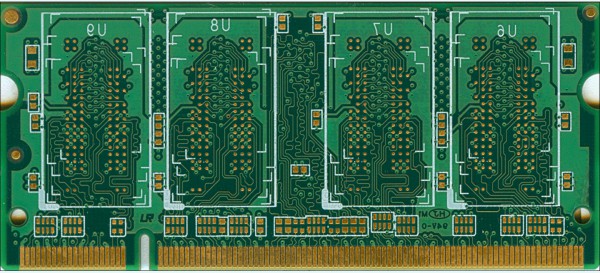
OSP(Organic solderability preservative) stands for organic solder-ability preservative (anti-oxidation), also known as copper shielding agent. Its essence is to act as a barrier between copper and air. The process flow of OSP is degreasing, secondary water washing, micro-erosion, secondary water washing, acid washing, deionized water washing, film-forming air drying, deionized water washing, and drying.OSP has three categories of materials: rosin (Rosin), active resin (Active Resin) and azole (Azole). Currently the most widely used is azole OSP. The azole OSP has been improved for about 5 generations, which are named BTA, IA, BIA, SBA and the latest APA.
In fact, OSP is not a new technology. It has actually been more than 35 years, which is longer than the history of SMT. OSP has many advantages, such as good flatness and no IMC formation between the copper of the pad, allowing direct soldering of solder and copper during soldering (good wettability), low-temperature processing technology, low cost (lower than HASL), Low energy use during processing, etc. OSP technology was very popular in Japan in the early days. About 40% of single-panel uses this technology, and nearly 30% of dual-panel uses it. In the United States, OSP technology also surged in 1997, from about 10% before 1997 to 35% in 1999.

So what is the difference between ordinary PCB and OSP PCB?
1) Different references:
OSP PCB is a process that conforms to the RoHS directive requirements for printed circuit board (PCB) copper foil surface treatment. The ordinary PCB board, also known as printed circuit board, is an important electronic component, a support for electronic components, and a carrier for electrical connection of electronic components.
2) Different processes:
OSP PCB is a chemically grown organic film on a clean bare copper surface. This layer of film has anti-oxidation, thermal shock resistance, and moisture resistance to protect the copper surface from rusting under normal conditions. The PCB is made using electronic printing.
3) Different uses
When OSP PCB is at high soldering temperature, this protective film must be easily removed by the flux, so that the exposed clean copper surface can be immediately combined with molten solder into a strong solder joint in a very short time. After the common PCB and electronic equipment use printed boards, due to the consistency of similar printed boards, errors in manual wiring are avoided, and automatic insertion or placement of electronic components, automatic soldering, and automatic detection can be achieved to ensure that The quality of electronic equipment improves labor productivity, reduces costs, and facilitates maintenance.
There are four main advantages of OSP PCB:
- Thermal stability. When compared with FLUX, which is also a surface treatment agent, it was found that the OSP had no oxidation after secondary heating at 235℃. The protective film is not damaged. Take two samples of OSP and FLUX respectively. At the same time, put 60℃. 90% in a constant temperature and humidity box. After one week, the OSP sample showed no significant changes. The sample surface of FULX shows small dots. That is because oxidation occurs after heating.
- Management simplicity. OSP process is relatively simple and easy to operate, the client can use any welding method to process it. No special treatment is required during circuit production. There is no need to consider the problem of surface uniformity. Which means don’t have to worry about the concentration of its medicine.
- Low cost. Because it only reacts with the bare copper part to form a non-sticky, thin and uniform protective film, so the cost per square meter is lower than other surface treatment agents. It can be said that in all surface treatment processes.
- Reduce pollution. OSP does not contain harmful substances that directly affect the environment, such as: lead and lead compounds, bromine and bromine compounds, etc., in the automatic production line, the working environment is good. Equipment requirements are not high.
- Downstream manufacturers are easy to assemble, adopting OSP for surface treatment, and the surface is smooth. When printing solder paste or pasting SMD components. Reduce the deviation of parts. At the same time reduce the probability of SMD spot welding.
Of course, OSP also has its shortcomings. For example, there are many types of actual formulas and different performances. In other words, the certification and selection of suppliers must be done well.The disadvantage of the OSP process is that the protective film formed is extremely thin and easy to scratch (or scrape), and must be carefully operated and operationally placed. At the same time, the OSP film (referred to as the OSP film on the un-welded connection pad) after multiple high-temperature welding processes will be discolored or cracked, affecting solder-ability and reliability.
