There are many places in PCB design that need to consider the safety distance. Here, it can be divided into two categories: one is electrical related safety distance, the other is non electrical related safety distance.
Electrical safety distance
1) Spacing between conductors
According to the processing capacity of mainstream PCB manufacturers, the distance between wires shall not be less than 4mil. The minimum line distance is also the distance from line to line and line to pad. From the production point of view, the larger the better, if possible, it is common to use 10mil as a routine.
2) Pad diameter and pad width
According to the processing capacity of mainstream PCB manufacturers, if mechanical drilling is used, the minimum pad diameter shall not be less than 0.2mm; if laser drilling is used, the minimum shall not be less than 4mil. The hole diameter tolerance is slightly different according to the different plates. Generally, it can be controlled within 0.05mm. The minimum pad width shall not be less than 0.2mm.
3) Distance between pads
According to the processing capacity of mainstream PCB manufacturers, the distance between pads shall not be less than 0.2mm.
4) Distance between copper sheet and plate edge
The distance between live copper sheet and PCB edge should not be less than 0.3mm. If it is a large area of copper, there is usually an internal contraction distance from the plate edge, which is generally set as 20MIL. In the PCB design and manufacturing industry, in general, for the sake of mechanical consideration of the finished circuit board, or to avoid the curling or electrical short circuit caused by the exposed copper sheet on the board edge, engineers often shrink the large-area copper block by 20MIL relative to the board edge, instead of laying the copper sheet to the board edge. There are many ways to deal with the shrinkage of copper skin. For example, the keepout layer is drawn on the edge of the plate, and then the distance between copper laying and keepout is set. This paper introduces a simple method, which is to set different safety distances for copper objects, such as setting the safety distance of the whole board to 10mil and setting the copper laying distance to 20MIL. The results show that the plate edge can be shrunk 20 ml. At the same time, the dead copper that may appear in the device is also removed.
Non electrical safety distance
1) Character width, height and spacing
No changes can be made to the text film during processing, but the line width of characters with d-code less than 0.22mm (8.66mil) or less will be thickened to 0.22mm. The width of character line is l0.22mm (8.66mil). The width of the whole character is w1.0 mm. The height of the whole character is h1.2mm. The spacing between characters is d0.2mm. When the text is less than the above standard, the processing and printing will be blurred.
2) Through hole to through hole spacing (hole edge to hole edge)
The via to via spacing (hole edge to hole edge) should be greater than 8 mil.
3) Distance from screen printing to pad
The pad is not allowed for screen printing. Because if the pad is covered with silk screen printing, the screen printing will not be tin coated when tin is applied, which will affect the installation of components. Generally, it is better to reserve a space of 8mil for the plate plant. If the actual area of PCB board is limited, the spacing of 4mil is barely acceptable. If the screen printing covers the pad carelessly in the design, the plate factory will automatically eliminate the silk screen part left on the pad to ensure the tin on the pad.
Of course, in the design of the specific situation of the specific analysis. Sometimes, the silk screen is deliberately placed close to the pad, because when the two pads are very close, the screen print in the middle can effectively prevent the solder joint from short circuiting during welding. This is another case.
4) 3D height and horizontal spacing on mechanical structure
When installing the components on PCB, it is necessary to consider whether there will be conflicts with other mechanical structures in horizontal direction and space height. Therefore, in the design, it is necessary to fully consider the adaptability of space structure between components, PCB products and product shell, and reserve a safe distance for each target object. The distance is considered to ensure that they do not conflict in space.
Several typical cases of safety distance design
1) Relationship between copper thickness, wire width and current
Under the normal process, the thickness of copper sheet is 18um, 35um, 50um, 70UM; and the thickness of more than 70UM is a special process. For PCB board with copper thickness of 150um, it is called thick copper plate. It mainly depends on electroplating and copper plating. If the copper thickness is not enough, it will be plated until the required thickness is reached. That is, plating treatment, this process is difficult, general manufacturers are not willing to make, and the cost is too expensive, not suitable for mass production. Suggestion: for the module wiring of extra large power supply, if the whole board does not need 150um, it can be considered to add tin manually or add additional high current copper conductor in parallel. This process is easy to operate and can also be produced in large quantities.
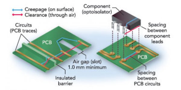
2) PCB clearance and creepage distance
PCB clearance refers to the shortest path between two conductive objects measured by air or between the boundary surface of conductive parts and equipment. It is also a common and commonly used spacing. Creepage refers to the shortest path between two conductive objects measured along the surface of the insulating material.
The trend of PCB design is always to reduce the size and increase the density of components in order to achieve miniaturization. Although new technology and new generation of components make all this possible, sometimes, especially when high-voltage circuit and common circuit are mixed, the key problems that PCB designers need to consider in design are more complex. With the current trend of miniaturization, high voltage systems must be placed on the same board, and designers must find solutions to implement these rules. This miniaturization presents some major challenges for designers, especially for hybrid technologies, where high-voltage circuits are part of the design, such as solar conversion and handheld medical imaging products. In the past, the high pressure plate was usually designed as a single board in a multi board system. Now, continuous drive for miniaturization means that we don't have space for multiple boards, and the number of designs using hybrid technology is increasing, where analog, digital and RF circuits are closely integrated with high voltage circuits. These high voltage circuits need to be in the form of increased electrical spacing and isolation, with additional design rules for the safety of the operator.
Almost all PCB design software tools refer to all gaps as clearance. In fact, all clearance parameters applied between conductive objects on an insulating surface, such as pad to pad, pad to wire and wire to wire spacing parameters, are crease, rather than clearance as we often say. The distance between conductive elements through air is clearance. There is no doubt that clearance will continue to be used in engineers' design and EDA tools as a gap in our usual sense (whether it is crease or clearance). However, in the application of high-voltage circuit, there is still a big difference between creepage and clearance in the traditional sense, which is what designers need to pay special attention to. Generally speaking, the creepage is always greater than or equal to the relevant clearance requirement.
3) Standards for calculating conductor spacing at various voltage levels
The proper distance between PCB lines is very important to avoid short circuit between electrical conductors. Unfortunately, there is no single solution to this problem. There are various industrial and safety standards that specify different bay requirements based on voltage, application, and other factors. When a product must be certified by a safety agency, each safety inspection agency has a series of standards to meet specific insulation requirements. In this case, it is convenient to find the required clearance. The level required depends on the location of the circuit. When considering the clearance and creepage requirements of a given design, the combination of pollution degree and insulation type should be considered. The degree of pollution usually refers to the content of dust, moisture and other particulate matter in the surrounding air or on the surface between high pressure nodes. The standard specifies functional, basic, supplementary, dual and reinforced insulation. These definitions of insulation are quite complex. The creepage standard also differs from these insulation classes.