When using Altium Designer to draw a PCB, you will find that there are solder mask layers and solder paste layers. What is the difference between them? These two layers are the most difficult to understand in Altium Designer.
PCB Solder Mask Layers (also known as solder resist) in Altium Designer
(1)It is an epoxy or photoimaging polymer layer used to protect copper on the PCB surface to prevent welding. The solder mask layer covers exposed copper traces on the surface of the printed circuit board. A solder mask acts as a PCB insulation, preventing corrosion, oxidation, or damage from chemical exposure. And modern printed circuit boards have very thin and fine pitch tracks and component pins that can cause short circuits after the soldering process. By using solder resist, this problem can be prevented.
PCB Paste Mask Layers (also known as solder resist) in Altium Designer
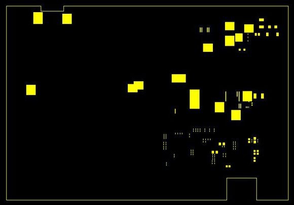
(1)This layer is used to make the stencil with punching holes, and the holes in the stencil correspond to the solder joints of the SMD devices on the printed circuit board. This is to help the device be soldered on the PCB, and the size of the Paste mask is the same as the size of the pads.
(2)When soldering surface mount devices, first cover the stencil on the printed circuit board (corresponding to the pads on the actual PCB), then print the solder paste, and then scrape off the excess solder paste with a blade, and finally remove the steel sheet. In this way, the solder paste is added to the pad of the SMD device, and then the SMD device is attached to the solder paste, and finally, the soldering of the SMD device is completed by a reflow soldering machine.
Issues to be aware of when generating paste mask from Gerber file by Altium Designer
(1)When Altium Designer creates a paste mask layer with a Gerber file. The paste mask data need be created with the dimensions of the solder mask determined so that it fits the expected openings and space.
(2)Dimensional requirements include specifying expansion metrics and creating shapes at each pad and via location that should be excluded from the coating. Once the shape is defined, the space is set to define the minimum gap & spacing in the board.
(3)When you apply the correct space in your PCB design rules, you can prevent accidental bridging during assembly.
Solder Mask Design Rules in Altium Designer
(1)There is a set of PCB rules and constraints editor in Altium Designer to design important PCB manufacturing rules for your solder mask. Because Altium Designer has a complete set of tools to specify your solder mask space. This rule allows you to design solder mask expansion or contraction for each pad and via.
(2)Altium Designer tools are a suite of design features for routing and high-speed layout linked together with automatic rule checking for layout and schematic. You can view your design, layout, and PCB fabrication in Altium Designer. So you can review your solder mask and paste mask layer from design to PCB manufacturing.
(3)Altium Designer allows you to accurately place components, verify PCB solder mask space, and examine your solder mask without using a separate program.
The meaning of each layer in Altium Designer
1.TOP LAYER: Designed for top layer copper foil traces. If it is a single panel, there is no such layer.2. BOMTTOM LAYER: Designed as bottom copper foil wiring.
3. TOP / BOTTOM SOLDER: The top/bottom layer is laid with a solder mask ink to prevent tin on the copper foil and maintain insulation.
4. TOP / BOTTOM PASTE: This layer is generally used to apply solder paste during the SMT reflow soldering process of chip components. It has nothing to do with the printed circuit board manufacturer's board. Keep the default during PCB design.
5. TOP / BOTTOM OVERLAY: Designed for various silk screen logos, such as component numbers, characters, trademarks, etc.
6. MECHANICAL LAYERS (mechanical layer): Designed as a PCB mechanical shape, the default LAYER1 is the shape layer. Other LAYER2 / 3/4, etc. can be used for mechanical dimensioning or special purposes. For example, LAYER2/3/4, etc. can be used when some boards need to make conductive carbon oil, but the purpose of this layer must be clearly marked on the same layer.
7. KEEPOUT LAYER: Designed as a prohibited wiring layer, many designers also use the PCB mechanical shape. If there are KEEPOUT and MECHANICAL LAYER1 on the PCB at the same time, mainly look at the shape integrity of these two layers. MECHANICAL LAYER1 shall prevail. It is recommended to use MECHANICAL LAYER1 as the shape layer when designing. If you use KEEPOUT LAYER as the shape, do not use MECHANICAL LAYER1.
8. MIDLAYERS (intermediate signal layer): Mostly used for multi-layer boards, and can also be used as a special purpose layer, but the purpose of this layer must be clearly marked on the same layer.
9. INTERNAL PLANES (inner electric layer): used for multi-layer board.
10. MULTI LAYER (through hole layer): through hole layer.
11. DRILL GUIDE (drilling positioning layer): The center positioning coordinate layer of the drilling of pads and vias.
12. DRILL DRAWING (drilling description layer): A description layer of the drilling hole size of the pad and the via.
Altium Designer Technology
1.Schematic Capture: Quickly capture your design intent with a rich set of wiring tools, design verification, transparent netlist creation, and variation management.2.Hierarchical & Multi-channel Design: Effortlessly design advanced electronics with intuitive navigation through all hierarchy levels, nets, and components.
3.Board Layout: Efficiently explore an optimal layout with intuitive board planning technology. Native 3D support, layer stack management, and high-end controls including etch factor and surface roughness models give you all the power you need in a single design space.
4.Data Management: Connect your team and design data together in one centralized location for easy access. A scalable platform meets the needs of growing companies, including design workspaces, project lifecycle and release management, and team collaboration.
5.Manufacturing Outputs: Ensure that your design is ready for production with support for every file that your manufacturer might need. We’ve got you covered with ODB++, IPC-2581, and Gerber X2 with a built-in CAM editor.
6.Fabrication Drawings: Instantly create detailed fabrication views of your board and components with Draftsman. MCAD-like dimensioning and intelligent reports make it easy to communicate design intent.
3D Gerber View
AiPCBA has designed a free online 3D Gerber file viewer tool. With this viewer, you can upload a Gerber file and have a 360-degree view of your PCB design. Using the AiPCBA Online 3D Gerber viewer, you can check for errors, and use the zoom function to inspect the board. You don't have to be a registered user to take advantage of this useful tool, and you don't need a high-processing computer to operate.
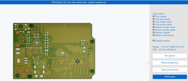
Allows you to see all layers in your design!
Allow you to see each layer of the Gerber file individually!
Allow you to see the size of your design!
Allows you to see your PCB design through different eyes!
Allows you to see your board as it will look from production!
Allows you to inspect it from any angle...like holding the finished board in your hand!
After viewing your Gerber file by AiPCBA online 3D Gerber Viewer, please send us your file for a free quote! Quote NOW!