The printed board should meet the size requirements specified in the design drawings, such as the perimeter, thickness, cutouts, openings, and slots of the board. Wire width error is within ±5%. Bonding IC can be accepted by 5261 within ±0.01mm; notch not exceeding 1/5 line width is acceptable; line gap error is acceptable within ±5%.
Aperture deviation is as follows:
When the aperture is ≤0.8 mm, the error between the aperture of the part and the designed aperture is 4102 between ±0.05mm.
When the aperture is> 0.8 mm, the error between the part aperture and the design aperture is between ±0.1mm.
Processing size (not more than ±1.5mm) and shape meet the requirements of design drawings. The minimum distance between the hole and the edge of the board: 1.0 mm; the dimensional tolerance of the hole and the edge is ±0.1mm; the tolerance of the hole position is ±0.10mm; the deviation standard of the partial design aperture percentage is 0.05 mm is ±0.05mm; drilling Tolerance standard for deviation holes of PCB board ≤0.076 mm; exposed copper foil lines or pads have a distance of more than 1.0 mm from the left and right sides of the board; copper foil lines have a distance of more than 1.0 mm from the V-groove or stamp connection hole of the tear plate.

For comprehensive design and production, we need to consider the following issues: 1. In principle, the inner diameter of the full through hole requires 0.2mm (8mil) and above, and the outer diameter is 0.4 mm (16mil) or more. In difficult places, the outer diameter must be controlled at 0.35 mm ( 14mil);
According to experience, the inner diameter and outer diameter of the commonly used via size of PCB generally follow X*2±2mil (X represents the inner diameter size). For example, the via diameter of 8mil can be designed as 8/14mil, 8/16mil or 8/18mil; for example, the via of 12mil can be designed as 12/22mil, 12/24mil, 12/26mil;
1) The design of BGA at 0.65 mm and above is recommended not to use buried blind holes, the cost will increase significantly. When buried blind holes are used, first-order blind holes are generally used (TOP layer-L2 layer or BOTTOM-negative L2. The inner diameter of the via hole is generally 0.1 mm (4mil) and the outer diameter is 0.25 mm (10mil).
2) Vias cannot be placed on pads smaller than the size of 0402 resistor pads; theoretically, the lead inductance on the pads is small, but during production, solder paste easily enters the vias, causing uneven solder paste and causing the device to stand The phenomenon of rising up (the phenomenon of standing monument. Generally recommended spacing is 4-8mil.
3) The distance between the via hole and the via hole should not be too close. Drilling is likely to cause holes. Generally, the hole spacing is 0.5 mm and above, 0.35mm-0.4mm is strongly avoided, and 0.3 mm and below is prohibited.

In addition to the heat dissipation vias, the vias of ≤0.5 mm need to be covered with oil (the inner diameter is 0.4 mm and the holes need to be plugged).
1) Especially for the devices with metal shells, in principle, no vias are punched under the body, and some plug holes punched with vias are covered with oil to avoid short circuit between the shell and the vias.
2) According to the production feedback of the board factory, it will often be mentioned that the via under the BGA is too close to the pad and the via needs to be moved. This situation is due to the fact that the vias are not equidistant from the BGA pads. Since the position of the vias and test holes under the BAG is not equidistant from the BGA pads, PCB designers do not pay attention to this, leading to continuous engineering problems, so cause hidden danger to welding quality. Therefore, we directly recommend punching to the center of the two pads, especially because the pitch of the PGA is small in the BGA. After punching, it is necessary to cover the via plug hole under the BGA to avoid short circuit of the BGA ball and tin.
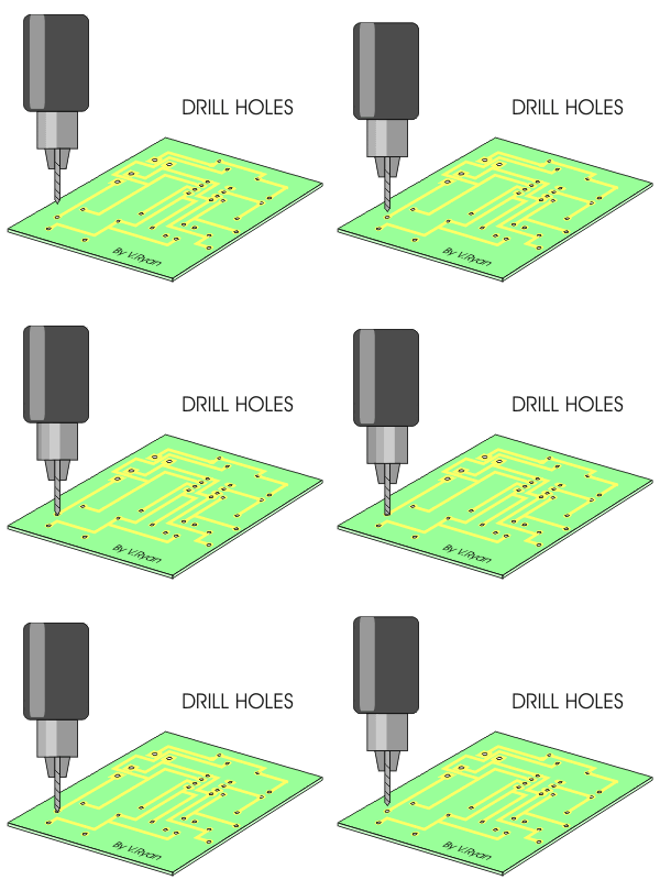
In the PCB production process, drilling is very important, not sloppy. Because drilling is to drill the required via holes in the copper clad plate to provide electrical connection and fix the function of the device. If the operation is improper, there is a problem in the process of drilling, the device cannot be fixed on the circuit board, it will affect the use at light weight, and the whole board will be scrapped, so the drilling process is very important.
