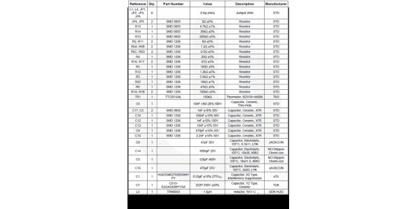
BOM is known as bill of materials, a file that describes the product structure in a data format that can be recognized by the computer and also an ERP insertion file. BOM enables the system to identify the product structure, and it also can convey the types of BOMs in various ERP systems of the enterprise.
If you plan to purchase parts yourself and then solder them on the PCB by hand, you may wonder why you need BOM in the beginning, and you just need to line up what you need from the top of the head. This is possible if you have a simple circuit board design with only a few common parts. However, once you start designing a circuit board consisting of dozens or even hundreds of parts, maintaining an organized component list will become a more reliable strategy than simply taking a note in your head.

There are many BOM formats out there, catering to different purposes and requirements, depending on what it will ultimately be used for. For now, there are some things that are often seen on a typical PCB BOM:Designator(The component symbols are the "letters" of this language.) / Component Value / Manufacturer’s Part Number(A new material number has been created and the manufacturer is specified in the material number) / Quantity / Description / Manufacturer’s Name / Package Type / Placement Method / Part link / Alternate Part number(When you replace a component in an assembly with another component, you can assign a new item number to the replaced component in the BOM and keep it on the same line as the removed component.).
Although PCB BOM bill production is not a technical task, it is also very important for the smooth commissioning and production of products and projects. Introducing basic BOM single design specification, generally speaking, device parameters (models), device descriptions, packages, tag numbers, quantities, and remarks are required. If they need to be delivered to purchase, they also need material numbers, brands, etc. Speaking of the BOM sorting rules, generally we arrange all components in the order of resistance, capacitance, inductance, diode, triode, IC, connector, and others, which called overall sequence. So how to make a PCB BOM normatively? Here are necessary steps we need:
1)Resistance sequencing method
The resistors are arranged internally from small to large, and special resistors need to be marked.
2)Capacitance sequencing method
The capacitors need to be classified within the capacitors (stacked capacitors, tantalum capacitors, electrolytic capacitors, etc.), and the electrical values within the classification are arranged from small to large, and special capacitors need to be marked.
3) Inductance sorting method
The inductance needs to be classified within the inductor (stacked inductor, winding inductor, power inductor, etc.), and the inductance value within the classification is arranged from small to large, and special inductors need to be marked.
4) IC arrangement method
Generally, they can be arranged in ascending order.
5) Connector
The connectors need to be classified within the connector, and then sorted within the classification from small to large.
6) Other
Other devices should also be classified according to the category, and then sorted within the classification from small to large.
Finally, don't forget to add information such as the title of the table and then you can get a standard PCB BOM.
