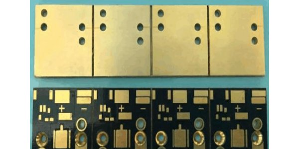
Copper PCB circuit board is the most expensive metal substrate, thermal conductivity is many times better than aluminum and iron substrate, suitable for high-frequency circuits and high - and low-temperature variation of the region and precision communication equipment heat and building decoration industry.
There are generally sinking gold - copper - based PCB, silver - plated copper - based PCB, tin - sprayed copper - based PCB, anti - oxidation copper - based PCB.
Copper PCB is one of the most expensive metal substrates. The thermal conductivity is many times better than that of aluminum substrates and iron substrates. It is suitable for high-frequency circuits and regions with large variation of high and low temperature, as well as for heat dissipation and building decoration of precision communication equipment.
1).There are generally sinking gold - copper - based PCB, silver - plated copper - based PCB, tin - sprayed copper - based PCB, anti - oxidation copper - based PCB.
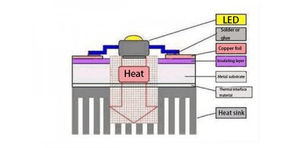
Copper-based PCB circuit layer is required to have a large current-carrying capacity, so thick copper foil should be used, the thickness is generally 35 m~280 m; Heat conduction and insulation layer is the core technology of copper-based PCB board. 2).The core heat conduction component is composed of aluminum oxide and silicon powder and epoxy resin filled polymer, with low thermal resistance (0.15), excellent viscoelasticity, thermal aging resistance, and the ability to withstand mechanical and thermal stress. Copper base PCB base metal is copper base PCB support components, requires high heat conductivity, usually copper, suitable for drilling, punching and shearing and cutting and other conventional mechanical processing, the metal layer (block) is mainly type cooling, shielding, grounding or role, because the performance of the copper and aluminum as well as the corresponding PCB can be differences in the processing technology, copper base PCB has more than aluminum substrate performance advantages.

Advantages of copper based PCB:
1). The thermal conductivity of copper PCB is twice that of aluminum PCB. The higher the thermal conductivity, the higher the heat conduction efficiency and the better the heat dissipation performance.
2). Due to the difference in the elastic modulus of copper and aluminum (the elastic modulus of copper is about 121,000 mpa, and the elastic modulus of aluminum is 72,000 mpa), the corresponding buckling degree and expansion and shrinkage of copper based PCB board will be smaller than that of aluminum substrate, and the overall performance is more stable.
3).copper PCB can be processed into metallized holes, but aluminum can not, the network of metallized holes must be the same network, so that the signal has a good grounding performance, and copper itself has weldability, so that the design of the structural parts can be selected for the final installation of welding.
4).Copper-based PCB of copper-based PCB board can etch fine graphics and process them into a boss shape. Components can be directly attached to the boss to achieve excellent grounding and heat dissipation effect;
Copper based PCB board design rules: due to the copper based PCB is thicker, the minimum diameter of the drilling tool must be 0.4mm, the line width spacing according to the copper foil thickness on the copper based PCB board to determine, the thicker the copper foil thickness, the need for the most thin line width is wider, the need for the minimum spacing must be greater.

Copper based PCB manufacturing method:
Substrate is the basic material for PCB manufacturing, in general, the substrate is copper-clad laminate, single, double-sided printed board in manufacturing is in the substrate material - copper-clad laminate, selective hole processing, electroless copper plating, electroplating copper, etching, and other processing, to obtain the circuit graphics.
When the substrate is installed, it is often necessary to punch holes and side openings on the substrate body, and complete the fixing and installation of the substrate through screws. In this way, it is not only possible to screw out the substrate when fixing, but also waste a lot of time to install, the installation efficiency is low.
1).Carving method:
This is the most straightforward method. Will design good copper foil graphics with carbon paper, carbon to copper foil surface, the use of hacksaw blade grinding system of special carving tool, directly on the copper clad plate along the edge of the copper foil graphics hard description, as far as possible to cut to the depth, and then tore off the graphics do not need the copper foil, and then drill hole with hand. The key of this method is: the intensity of description should be enough; To remove excess copper foil, begin at the edge of the plate and, when done well, gradually tear off the foil in pieces, using small, pointed nose tongs. Some small circuit experimental version is suitable for this method.
2).Manual description:
It is to use the pen to print graphics directly on the copper clad plate, and then chemical corrosion and other steps. This method seems simple, practical operation is not easy! Today's electronic components are small in size, pin spacing is smaller (mm), copper foil line is also fine, and the lines are difficult to modify, to draw such a board is entirely up to you. The lesson is: both "paint" and the choice of brush are critical. I myself have used red nail polish in a medical syringe to depict the circuit board, which works fine, but the tip of the needle needs to be properly mached; Some people also introduced the use of paint tablets dissolved in anhydrous alcohol, the use of a platypus pen sketch, the specific method is as follows:
(1).Will be the paint (namely shellac, chemical raw materials shop to sell), dissolve in three parts of anhydrous alcohol, and stir properly, after all its dissolved, drop a few drops of medical violet (gentianzi), make it appear a certain color, stir evenly, can be used as a protective paint to describe the circuit board.
(2).Apply polish copper plate with fine sand paper first, and then use the drawing pen drawing instrument (or ink drawing pen used to draw graphics on compass), paints, adjust the stroke weight of nut drawing pen, the stroke weight is adjustable, and can borrow ruler, set square depicts a very fine line, and as the line is smooth, uniform, margin serrate, give a person the sense with smooth and fluent; At the same time, you can also write Chinese characters, English, pinyin or symbols on the circuit board of the free place to depict the line, if to the surrounding infiltration, is too small, you can add a little paint; If you can't get started, it's too thick, and you need a few drops of alcohol. Just use a small stick (matchstick), make a small cotton swab, dip in a bit of alcohol, can be easily erased, and then redraw. Once the circuit board is mapped, it can be corroded in a solution of ferric chloride. After circuit board corrods good, go lacquer is very convenient also, dip in with cotton ball on anhydrous alcohol, can wipe off protective lacquer, slightly one air is dry, can besmear subsequently on rosin water is used.
(3).As a result of alcohol volatilization is fast, the protective paint that made up should be put in small bottle (if inkwell) seal is saved, after using, do not forget to close bottle lid, if be used next time, discover concentration became thick, want to add right amount to do not have water alcohol only can.
