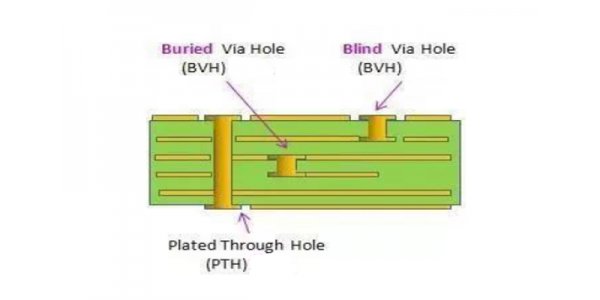
The most effective way to improve the PCB density is to reduce the number of through holes, and precisely set up blind holes, buries to achieve.
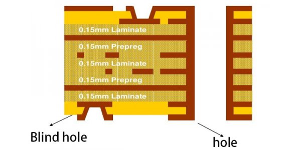
A: compared with through hole, through hole refers to the hole through which all layers are drilled. Blind hole is non-through hole. (as shown in the drawing, for example: through hole, blind hole and buried hole).

B: BLIND HOLE: BLIND HOLE, BURIED HOLE (the outer layer cannot be seen); C: from the production process: the blind hole is drilled before pressing and closing。
The through hole is drilled after pressing.
2. Production method:
A: drill tape:
(1) selection of reference point: select the through hole (that is, a hole in the first drill band) as the unit reference hole.
(2) : for each blind hole drilling belt, a hole should be selected and the coordinates of its relative unit reference hole should be marked.
(3) : note that which drilling belt corresponds to which layer: the unit orifice diagram and the drilling nozzle table should be indicated, and the names before and after should be indicated.
Consistent; A, b, c, and 1st, 2nd in front of the porthole chart cannot appear.
Note that when the laser hole is jacketed with the inner buried hole, that is, the holes of the two drill belts are in the same position, the position of the laser hole should be moved to ensure the electrical connection.
B: production of PNL plate edge process hole: ordinary multi-layer plate: no drilling in the inner layer;
(1) rivet gh, aoi gh, et gh are all etched after the plate;
(2) : target hole (drilling gh) CCD: outer layer need to pick copper, X-ray machine: directly, and pay attention to the minimum length of 11 inches.
Blind hole plate:
All tooling holes are drilled out, pay attention to rivets to avoid alignment deviation. The production of PNL plate edge drilling, in order to distinguish each plate.
3. Film modified:
(1) film for positive film, negative film:
General principle: the thickness of the plate is greater than 8mil (without copper connection); The plate thickness is less than 8mil (without copper connection).
When the thick line gap valley is large, the copper thickness at d/f should be considered instead of the bottom copper thickness. 5mil for blind hole ring, not 7mil.

The inner layer independent pad corresponding to the blind hole shall be retained. Holes cannot be made without ring.
4. Process:
Buried-hole plate and common double - panel practice.
Blind orifice plate, that is, one side is the outer layer:
Positive film process: single side d/f is required, and attention should be paid not to roll the wrong side (when the copper on the double side is inconsistent); When d/f is exposed, the smooth copper surface is covered with black tape to prevent light transmission.
Because the blind hole plate made more than twice plate electricity, electricity, the finished product is extremely easy plate thickness, so pay attention to the control plate thickness copper thickness, etching after indicating the copper plate thickness range.
After pressing the plate, use the X-ray machine to punch the multilayer plate with the target hole.
Negative film process: for thin plate (< 12mil connect copper > because it can not be produced in the drawing, must be produced in the hydro-gold drawing, and hydro-gold drawing can not be divided surface current, so can not.
According to the mi requirements to do one side of the current or small current. Such as the positive sheet process, often lead to a single side of copper thickness super thick, resulting in etching difficulties, thin line phenomenon, so this kind of plate.
Go negative:
5. The drilling order of through hole and blind hole is different, and the deviation is not consistent
The blind orifice plate is easy to be deformed, and it is difficult to control the position of the multi-layer plate and the distance between the pipe and the horizontal material, so only the horizontal material or only the straight material is opened when the material is opened.
The andante flow of this kind of plate should pay attention to use resin to seal the hole before making the line to avoid the line to cause greater damage.

PCB blind hole manufacturing:
Blind hole refers to the connection between the outermost circuit in the PCB and the adjacent inner layer with an electroplating hole. Because the opposite side cannot be seen, it is called blind hole. In order to increase the space utilization between the layers of the board circuit, blind holes are used. A blind hole is a pass hole to the surface of a printed board.
The blind hole is located on the top and bottom surface of the circuit board and has a certain depth, which is used for connection between the surface line and the inner line below. The depth of the hole generally has a specified ratio (aperture). This production method needs special attention, the drilling depth must be just right, if you do not pay attention to the hole will cause plating difficulties. Therefore, few factories will adopt this method of production. In fact, it is possible to drill holes in the circuit layers that need to be connected in advance, and finally bond them together, but it requires a more precise positioning and alignment device.

This manufacturing process cannot be achieved by the way of drilling after the bonding of the circuit board, but the drilling operation must be carried out at the time of the individual circuit layer, after the partial bonding of the inner layer, electroplating treatment, and finally all bonding. Because the operation process is more laborious than the original through hole and blind hole, so the price is also the most expensive. This process is usually used only for high-density circuit boards, increasing the space utilization of other circuit layers.
In printed circuit board (PCB) production process, drilling is very important. Drilling is simply understood as drilling the required hole in the copper clad plate, with the function of providing electrical connections, fixed devices. If the operation is not correct leading to the hole process problems, devices can not be fixed on the circuit board, the use of the circuit board will affect the light, heavy will let the entire board is scrapped, so drilling this process is very important.
