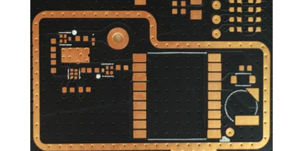
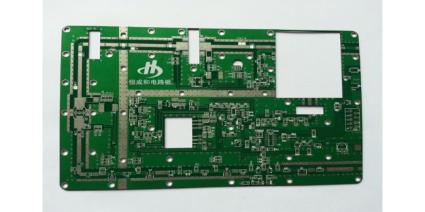
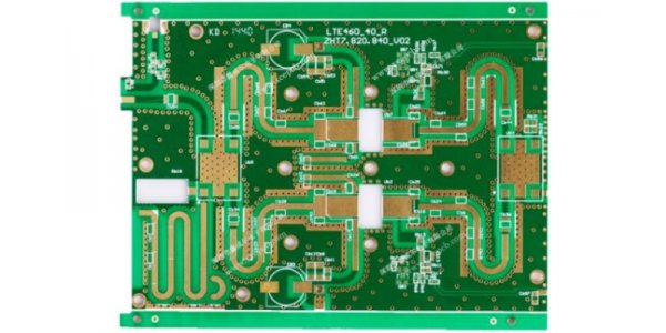
1.High-frequency PCB definition:
Embedded radiators, pure polytetrafluoroethylene (PTFE) multilayer circuits, Rogers PCB materials, designed and manufactured using fusion or hybrid materials (FR4 and PTFE), have become the standard technology for VARIOPRINT, and are widely implemented and have the stability of daily control process parameters.High-frequency electronic devices are the trend today, especially in wireless networks. The rapid development of satellite communications, information products to high - speed, high - frequency. Therefore, the development of new products always requires the use of high-frequency substrates, satellite systems, mobile phone receiving base stations, etc., and these communication products must use high-frequency PCB.

2.High-frequency PCB features:
1).DK should be small and stable enough, usually the smaller the better. High DK may cause signal transmission delay.2). DF should be small, which mainly affects the quality of signal transmission. A smaller DF can correspondingly reduce signal loss.
3). The coefficient of thermal expansion should be the same as that of copper foil as far as possible, because the difference will lead to the separation of copper foil during the change of cold and heat.
4). In the humid environment, the water absorption rate must be low and high, which will affect DK and DF.
5). Heat resistance, chemical resistance, shock resistance and peel resistance must be good.
In general, high frequencies can be defined as frequencies above 1GHz. Currently, polytetrafluoroethylene (PTFE) materials are widely used in high-frequency PCB manufacturing, also known as Teflon, with frequencies usually higher than 5GHz. In addition, the FR4 or PPO substrate can be used for product frequencies between 1GHz and 10GHz. The three high-frequency substrates have the following differences:
1).Regarding the lamination cost of FR4, PPO and Teflon, FR4 is the cheapest and Teflon is the most expensive. In terms of DK, DF, water absorption and frequency characteristics, teflon is the best. When the frequency of product application is higher than 10GHz, we can only choose Teflon PCB substrate to manufacture. Obviously, Teflon's performance is much better than other substrates, but Teflon substrates have the disadvantages of high cost and high heat resistance. To improve the rigidity and heat resistance of PTFE, a large amount of SiO2 or glass fiber is used as the filling material. On the other hand, since the molecular inertia of PTFE material is not easy to bond with copper foil, special surface treatment is needed on the combination side. For combined surface treatment, it is common to use chemical etching or plasma etching on the surface of PTFE to the surface roughness or to add an adhesive film between PTFE and copper foil, but these may affect the dielectric properties.

3.Advantages of high-frequency PCB:
1). High-frequency circuit boards with small dielectric constant will have small loss, and advanced induction heating technology can achieve the heating requirements of the target, with very high efficiency. Of course, while paying attention to efficiency, it also has the characteristics of environmental protection, which is very suitable for the development direction of today's society.2). The transmission speed is inversely proportional to the square root of the dielectric constant, which means that the smaller the dielectric constant, the faster the transmission speed. This is the advantage of high-frequency circuit board, it USES a special material, not only to ensure the dielectric constant is small, but also maintain the stability of operation, for signal transmission is very important.
3) is widely used in various industries for precision metal material heat treatment requirements of high frequency circuit board, in the field of the process, not only can realize the depth of different parts of heat, but also according to the characteristics of the local key heating, both the surface and deep, centralized or decentralized heating mode, can be easily accomplished.
4) dielectric constant and medium, there will be certain requirements on the environment, especially in the south, wet weather will seriously affect the use of circuit boards. High frequency circuit boards made of very low absorbent materials can challenge such an environment, but also have the advantages of resistance to chemical corrosion, resistance to moisture and high temperature, and great peeling strength, let the high frequency circuit board play a powerful performance.

4).In SMT SMT processing plants, high-frequency PCB usually has high frequency laminate which is difficult to manufacture. This is because they need to maintain the heat transfer of the application in order for the product to work properly. The utility model provides the high frequency circuit board, the hollow core board slot opening and the opening on the edge of the guard has to stop the flow gel, in this way, the core board and on the adhesion of the surface and the lower surface of the copper clad laminates won't flow glue into the hollow grooves in the adhesive bonding can complete operation in a short period of time, the existing technology subject to secondary pressure to achieve high frequency circuit boards, high frequency circuit board of the utility model structure is simple, low cost, easy to manufacture.
4.Key points of high frequency PCB design:
High frequency circuits often have high integration and high wiring density. The use of multilayer circuit board is not only necessary for wiring, but also an effective way to reduce interference. In the PCB layout stage, a reasonable selection of a certain number of printed circuit board size can make full use of the middle layer to set the shielding, to achieve better near-grounding, effectively reduce parasitic inductance, shorten transmission length by reducing the crosstalk signal, etc., all of these methods are conducive to the reliability of high-frequency circuit. According to the data, the noise of the four-layer board is 20dB lower than that of the double-layer board. But there are problems. The higher the number of PCB half layers, the more complex the manufacturing process and the higher the unit cost. This requires us to select an appropriate number of PCB boards for PCB layout. Correct component layout planning and correct wiring rules to complete the design.
