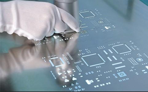
What is SMT Stencil?
SMT Stencil It is a special mold for SMT, its main function is to help the deposition of solder paste, and the purpose is to transfer the exact amount of solder paste to the exact position on the empty PCB. It is used to quantitatively dispense solder paste or patch glue, and it is a key tool to ensure the quality of printed solder paste/patch red glue.
The importance of SMT Stencil in the PCB Assembly
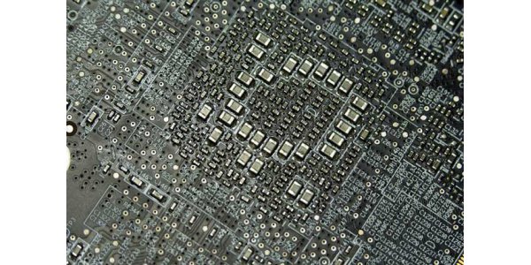
1)The function of the stencil is to print the semi-liquid semi-solid tin paste on the PCB circuit board. Except for the power supply board, most of the current popular circuit boards use the surface mount and SMT chip processing technology. There are many label pads on the PCB, that is, pads without vias, and the holes on the stencil are exactly the corresponding component patch pads on the PCB. Hand-printed solder paste is to use horizontal printing to print semi-liquid and semi-solid tin paste on the PCB through the holes on the stencil, then pick and place the components on the pick and placement machine, and then go through reflow soldering.
2)The SMT Stencil process is indispensable in the SMT assembly process. The thickness of the stencil, the size of the opening, the shape of the opening, and the state of the inner wall of the opening determine the printing amount of the solder paste, so the quality of the stencil will directly affect the solder paste. If the solder paste is insufficient or too much, it will cause false soldering, tin connection, and other conditions. It takes time to solder and cleans up again, which directly affects the time to complete the PCB assembly.
3)Stencil production is very important for the SMT process, it directly determines whether the tin on each pad is uniform and full, which will affect the soldering reliability of SMT components after reflow soldering. Generally speaking, the opening of the stencil requires careful analysis of the characteristics of each PCB. For some circuit boards with high precision and high-quality requirements, laser stencils must be used. SMT engineers need to discuss and confirm the process flow and then adjust the openings appropriately. The aperture guarantees the tinning effect.
In AiPCBA you don’t need to worry about the stencil quality problem. Because AiPCBA has over 7 years of knowledge and combined experience in rendering high tech PCB assembly services, PCB manufacturing services and different PCB assembly technologies like Through-hole (THT) and Surface Mount (SMT). Learn more about AiPCBA.
Types of SMT stencil
1)Laser Stencil: It is currently the most commonly used in the SMT stencil industry. It is directly produced by data files, which reduces production errors. This SMT stencil opening position accuracy is extremely high, the whole process error is less than or equal to ±4μm. The opening of the SMT stencil has geometric figures, which is beneficial to the printing and forming of the solder paste.
2)E.P.Stencil: It is after laser cutting, and treated by electrochemical method to improve the hole wall of the opening. This stencil has smooth hole walls and is especially suitable for ultra-fine pitch QFP/BGA/CSP. It can reduce the wiping times of the SMT template and greatly improve work efficiency.
3)Step Stencil: Due to the different requirements for the amount of solder paste when welding various components on the same PCB, the thickness of some areas in the same SMT stencil is required to be different, which results in the STEP-DOWN&STEP-UP process template. It can locally thin the stencil to reduce the amount of tin when soldering the specific components.
Types of SMT Stencil production processes
1)Chemical EtchingProcess flow: PCB data file → film production → exposure → development → etching → steel sheet cleaning
Features: One-time molding, faster speed, cheaper price.
Disadvantages: Not enough accuracy, not environmentally friendly, and have been gradually eliminated.
2) Laser Cutting
Process flow: PCB film production → take coordinates → data file → data processing → laser cutting → polishing
Features: high precision of data production, little influence of objective factors, trapezoidal opening is good for demoulding, precision cutting can be done, the price is moderate.
Disadvantages: cutting one by one, the production speed is slower.
3) Electroforming
Process flow: coating a photosensitive film on the substrate → exposure → development → electroforming nickel → forming → steel sheet cleaning
Features: The hole wall is smooth, especially suitable for the ultra-fine pitch steel mesh manufacturing method.
Disadvantages: the process is difficult to control, the production process is polluting, and it is not conducive to environmental protection, the production cycle is long and the price is too high.
Stencil opening design
The opening design of the stencil should consider the release property of the solder paste, which is determined by three factors:1)The aspect ratio/area ratio of the opening.
2)The geometry of the side wall of the opening.
3)The smoothness of the hole wall.
Because the laser stencil is very cost-effective, here we focus on the opening design of the laser stencil.
Of the three factors, the latter two are determined by the manufacturing technology of the steel mesh, so we consider the first factor more.
First, we know the aspect ratio and area ratio.
1)Aspect ratio: the ratio of opening width to stencil thickness.
2)Area ratio: The ratio of the opening area to the cross-sectional area of the hole wall.
Generally speaking, to obtain a good demoulding effect, the width-thickness ratio should be greater than 1.5, and the area ratio should be greater than 0.66.
When should the aspect ratio be considered and when should the area ratio be considered? Generally, if the length of the opening does not reach 5 times the width, the area ratio should be considered to predict the release of the solder paste, and the aspect ratio should be considered in other cases.
The following are examples of openings for some components:
|
Component Type |
PITCH |
Pad width |
Pad length |
Opening width |
Opening length |
Stencil thickness |
Aspect ratio |
Area ratio |
|
QFP |
0.635mm |
0.35mm |
1.50mm |
0.30-0.31mm |
1.45mm |
0.15-0.18mm |
1.7-2.1 |
0.69-0.85 |
|
QFP |
0.50mm |
0.254mm |
1.25mm |
0.22-0.24mm |
1.20mm |
0.12-0.15mm |
1.5-2.0 |
0.62-0.83 |
|
QFP |
0.43mm |
0.20mm |
1.25mm |
0.19-0.20mm |
1.20mm |
0.10-0.12mm |
1.6-2.0 |
0.68-0.85 |
|
QFP |
0.30mm |
0.18mm |
1.00mm |
0.15mm |
0.95mm |
0.07-0.10mm |
1.5-2.1 |
0.65-0.93 |
|
BGA |
∮1.27mm |
∮0. 8mm |
∮0. 75mm |
0.15-0.18mm |
1.0-1.25mm |
|
|
|
|
BGA |
∮1.0mm |
∮0.5mm |
∮0. 48mm |
0.12-0.15mm |
0.80-1.0mm |
|
|
|
|
uBGA |
∮0.8mm |
∮0.4mm |
∮0. 40mm |
0.12-0.15mm |
0.67-0.83mm |
|
|
|
|
uBGA |
∮0.8mm |
∮0.4mm |
□0. 38mm |
□0. 38mm |
0.12-0.15mm |
0.63-0.79 |
|
|
|
uBGA |
∮0.5mm |
∮0.25mm |
□0. 28mm |
□0. 28mm |
0.08-0.10mm |
0.70-0.86 |
|
|
|
0402 |
0.5mm |
0.65mm |
0.48mm |
0.635mm |
0.10-0.12mm |
1.4-1.37 |
|
|
|
0201 |
0.25mm |
0.40mm |
0.235mm |
0.38mm |
0.08-0.10mm |
0.73-0.91 |
|
|
The Notes of using the SMT Stencil
1)Take it lightly.2)The Stencil should be cleaned before use to remove the dirt carried during transportation.
3)The solder paste or red glue should be stirred evenly to avoid blocking the opening.
4)Adjust the printing pressure to the best. It is best when the pressure is adjusted to the extent that the scraper can just scrape the solder paste on the stencil.
5)After the scraper completes the work, it is best to stop for 2 to 3 seconds before demoulding, and the demoulding speed should not be too fast.
6)Do not hit the stencil with hard objects or sharp knives.
7)After the production, the stencil should be cleaned in time, returned to the packing box, and placed on a special storage rack.
Influence factors of SMT Stencil
1)Production processThe best process is electropolishing after laser cutting. Chemical etching and electroforming are subject to errors, such as film, exposure, and development, and electroforming is also affected by substrate unevenness.
2) Selection of materials
The screen frame must be able to withstand a certain program of relays and have a good levelness; it is best to use a polyester screen for the screen, because it can maintain the tension and stability for a long time; and the steel sheet should preferably be 304, Will be more conducive to solder paste rolling than the mirror.
3) Design of the opening
The design of the stencil opening has the greatest influence on the quality of the stencil. The design of the opening must take into account the manufacturing process, width-to-thickness ratio, area ratio, and experience values.
4) Completeness of production materials
The more complete the information, the better. At the same time, when there are several kinds of data coexisting, it should be emphasized which one prevails. In addition, the stencil produced by the data file can minimize the occurrence of errors.
5) Use of printing methods
The correct printing method can maintain the quality of the stencil and increase its life. Conversely, improper printing methods, such as too much pressure, and the stencil or PCB is not level during printing, will cause the stencil to be damaged to varying degrees.
6) Methods of cleaning
Solder paste is particularly easy to cure. If the solder paste or tin powder on the stencil is not cleaned in time, the opening of the stencil will be blocked, and reprinting will cause difficulties and errors. Therefore, after the stencil is removed from the machine or the solder paste is not printed on the printer for 1 hour, it must be cleaned in time.
7) Storage conditions
Different materials will have different storage environments. The steel mesh should also be stored in a specific storage place. It should not be placed randomly, so that the steel mesh can be protected from accidental injury. At the same time, the steel nets should never be stacked together randomly. This is not beautiful and bad, and it is possible to bend the net frame.
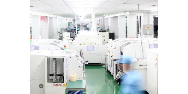
PCB Manufacturing and PCB Assembly in AiPCBA
AiPCBA can provide PCB manufacturing and assembly service. We have customers from different industries in terms of cost-effectiveness, quality, delivery and any other requirements. From PCB layout to PCB prototyping, mass manufacturing, and then PCB assembly, electronic box assembly services, our printed circuit boards are widely used in robotics, medical, automotive, communications, industrial and consumer electronics products.
Whether your technology includes Surface Mount (SMT), Through-hole, or a mixed technology for single or double-sided boards in small quantities, prototypes, or large production runs, AiPCBA has the ability to provide for all of your contract electronics manufacturing needs.
We have strong quality control system and all the certificates such as TS16949, UL, RoHS, CE, ISO, etc.. For PCB, we have Flying Probe Test and E-Testing. For PCBA, we have IQC, AOI, Function Test, QA. These are basic but very important factors for PCB industry.
Feel free to contact us if you have any inquiry! Quote now in AiPCBA!