PCB dry film refers to the raw materials used to make circuit. Dry film is a kind of polymer compound, which can produce a kind of stable substance attached to the board surface after ultraviolet radiation, so as to achieve the function of blocking electroplating and etching. If it is a circuit board with holes, the choice of dry film will be more appropriate. While the environment is not easy to control if the quality of the film is not easy to maintain. The dry film is easy to operate, but it is easy to keep clean and easy to operate without baking, so it is more favorable for use. However, for thin film thickness, especially the thickness below 15 μ m, dry film is not easy to achieve.

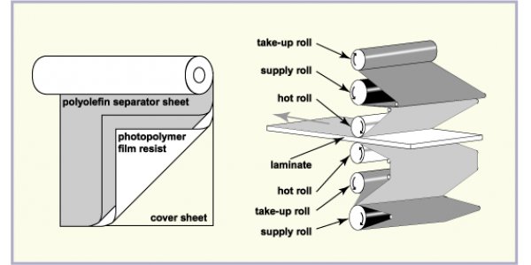
The dry film thickness ranges from 1.0 to 2.0 mils. For elaborate line resolution, thin films are desirable. If broaching is required, thick film is more suitable. The dry film is usually provided in roll form on a 3-inch (i.d.) core with a width of 6 to 27 inches. They are three-layer sandwich structures. A photopolymer barrier layer consists of a bottom layer of polyethylene (PE) film as a separator and a top layer of polyester or polyester film as a protective layer. In addition to protection, the top plastic film acts as an oxygen barrier to limit the amount of oxygen migrating into the resist film during exposure. During lamination, the laminating machine will remove the backing film. After exposure, the top film should be in contact with the photoresist for at least 15 minutes. It can only be removed before development. The dry film is sensitive to UVA radiation in the range of UV-A. Different brands have slightly different configurations.

Dry film imaging of PCB is a method to expose the photoresist coated on the substrate of printed circuit board to change its hardness, adhesion, solubility and physical properties, and form an image after development. PCB manufacturing photochemical image transfer photoresist has two main categories, one is photoresist dry film (referred to as dry film), its commodity is a photosensitive imaging photosensitive ink, the other is liquid photoresist, it also includes ordinary liquid photoresist and electrodeposition liquid photoresist (ED resist), ED resist is a water-based emulsion. Photoresist is the cornerstone of modern printed circuit industry. Photoresist dry film has the characteristics of simple process flow, low requirement of cleanliness and easy operation.

Since its appearance, dry film imaging of PCB has been welcomed by printed circuit enterprises. After several improvements and development, it has become the mainstream product in the film imaging process of printed circuit manufacturing. Before the appearance of photoresist dry film, liquid photoresist was an important material for imaging technology at that time. Because the thickness is not easy to control, the operation speed is slow, and the defects of the plate surface caused by the cleanliness and treatment of the process environment limit its use. After the advent of membrane, it was once replaced by dry film process. However, in recent years, with the development of electronic products in the direction of thin, small and dense, the pressure to reduce the price of printed circuit enterprises, the emergence of new high-resolution liquid photoresist, and the continuous large-scale production capacity of liquid photoresist coating equipment, make it in the field of printed circuit film imaging again.
