The best Multilayer PCB design software at present
Posted: May 14, 2022
By: Bonnie
The best Multilayer PCB design software at present is a list recommended by several hardware engineers, mainly including Altium design, eagle and OrCAD. Multilayer PCB Manufacturing Process
Multisim is a Windows-based simulation tool launched by National Instruments (NI) Co., Ltd., suitable for board-level analog/digital circuit board design. It includes graphical input of circuit schematics, circuit hardware description language input, and has rich simulation analysis capabilities.
Engineers can use Multisim to interactively build circuit schematics and simulate the circuit. Multisim refines the complex content of SPICE simulation so that engineers can quickly capture, simulate and analyze new designs without knowing in-depth SPICE technology, which also makes it more suitable for electronics education. Through Multisim and virtual instrument technology, PCB design engineers and electronics educators can complete a complete integrated design process from theory to schematic capture and simulation to prototype design and testing.
Provides a method of converting schematic diagrams and simulation data to other programs, and can output schematic diagrams to PCB wiring.
Altium Designer 20 represents decades of innovation and development dedicated to creating a truly unified design environment - one that enables users to effortlessly connect with every facet of the PCB design process.
Striking the perfect balance between power and ease of use, Altium Designer has secured its position as the most widely-used PCB design solution on the market.
The unified feature of Altium Designer allows design data to be seamlessly transferred from one design domain to the next. But first of all, the intuitively felt curve pattern of a large amount of data and information that is deeply expanded will show a huge obstacle to this productivity-enhancing environment and its rich functions. Therefore, the unique document core space of Altium Designer provides all the information needed to quickly start and run the software. From the high-level overview and step-by-step deployment, to the comprehensive coverage of all the fragmentary functions and information resources provided through the intuitive software interface, the Altium Designer documentation truly provides a readily available "knowledge tree" structure.
Features
Advanced wiring technology
Support trimming rigid-flex circuit board design
Powerful data management tools
The ECAD library contains more than 300,000 ready-to-use components
Powerful design reuse tool
Real-time cost estimation and tracking
Dynamic Supply Chain Intelligence
Native 3D visualization and gap inspection
Flexible release management tools
All these functions and the entire design process are implemented through a unified design environment (the only peer).
SOLIDWORKS PCB enables the productivity you need to design Printed Circuit Boards (PCBs) quickly along with unique, collaboration between electrical and 3D mechanical design teams. It offers a clear advantage where ECAD-MCAD collaboration is critical for overall success of electronic product design.
Function:
Rigid-Flex Design
Design and Data Management
ECAD-MCAD Design Collaboration
PCB Design Engine
Modern Schematic Entry
Streamlined Interface
Managed ECAD-MCAD ECO Process
Real-time 3D Clearance Checking
Mixed-Mode SPICE 3f5 Simulator
Supplier Links/Search
Version Control
Component Parametric Database Support
SOLIDWORKS File Support
Design Commenting and Revision Managemen
 price: Free
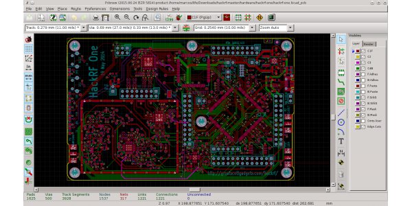
KiCad (pronounced "Key-CAD") is a free software suite for electronic design automation (EDA). It facilitates the design of schematics for electronic circuits and their conversion to PCB designs. KiCad was originally developed by Jean-Pierre Charras. It features an integrated environment for schematic capture and PCB layout design. Tools exist within the package to create a bill of materials, artwork, Gerber files, and 3D views of the PCB and its components.
The KiCad suite has five main parts:
KiCad – the project manager.
Eeschema – the schematic capture editor.
Pcbnew – the PCB layout program. It also has a 3D view.
GerbView – the Gerber viewer.
Bitmap2Component – tool to convert images to footprints for PCB artwork.
Key Benefits
Speeds designs from placement and routing through to manufacturing
Includes powerful features such as design partitioning, RF design capabilities, and interconnect design planning
Production proven to increase productivity and help engineers quickly ramp up to volume production
TÜV SÜD “Fit for Purpose – TCL1” certified to meet ISO 26262 automotive functional safety requirements
Features
Provides a scalable, full-featured PCB design solution
Enables a constraint-driven design flow to reduce design iterations
Integrated DesignTrue DFM technology providing real-time DFM checks
Provides a single, consistent, front-to-back constraint management environment
Minimizes design iterations and lowers overall cost for flex and rigid-flex designs with advanced rigid-flex design capabilities
Enables dynamic concurrent team design capability to shorten design cycle by dramatically reducing time spent on routing, tuning, and optimization of signals
Delivers an integrated RF/analog design and mixed-signal design environment
Provides interactive floorplanning and component placement
Provides design partitioning for large, dispersed development teams
Enables real-time, interactive push/shove etch editing
Allows real-time plowing/healing with dynamic shape technology
Manages net scheduling, timing, crosstalk, layer set routing, and geometric constraints
Provides proven PCB router technology for auto-routing of random signals
Enables hierarchical route planning to accelerate design completion
Shortens interconnect planning and routing time for dense designs with high-speed interfaces
Provides a comprehensive, powerful, easy-to-use suite of tools to assist designers with an efficient and successful handoff to manufacturing:
DFM Checker for signoff against company/manufacturing-partner-specific rules
Documentation Editor for reducing fabrication and assembly documentation time up to 70%
Panel Editor for communicating assembly panel design intent to manufacturing partners
Outputs design data in a variety of manufacturing formats
 price:
EAGLE is a scriptable electronic design automation (EDA) application with schematic capture, printed circuit board (PCB) layout, auto-router and computer-aided manufacturing (CAM) features. EAGLE stands for Easily Applicable Graphical Layout Editor (German: Einfach Anzuwendender Grafischer Layout-Editor) and is developed by CadSoft Computer GmbH. The company was acquired by Autodesk Inc. in 2016.
 price:Not Free
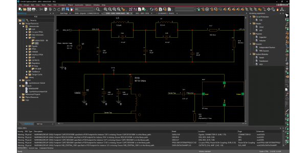
OrCAD is a set of electronic design automation package software on personal computers, which is specially used for electronic engineers to design circuit diagrams and related diagrams, design printed diagrams for printed circuit boards, and circuit simulation.
ORCAD Capture (hereinafter referred to as Capture) is a circuit design tool based on Windows operating environment.
Using Capture software, it is possible to draw circuit schematics and provide continuous simulation information for the production of PCBs and programmable logic designs. As the industry standard PCB schematic input method, OrCAD Capture is one of the most popular schematic input tools in the world today, with a simple and intuitive user design interface. OrCAD Capture CIS has a powerful component information system that can manage component databases online and centrally, thereby greatly improving the efficiency of circuit design. OrCAD Capture provides a complete and adjustable schematic design method, which can be effectively applied to PCB design creation, management and reuse. Combining schematic design technology and PCB layout technology, OrCAD can help designers grasp the design intent from the beginning. Whether it is used to design analog circuits, complex PCBs, FPGAs and CPLDs, schematic modifications of PCB revisions, or to design hierarchical modules, OrCAD Capture can provide designers with fast design input tools. In addition, OrCAD Capture schematic input technology allows designers to input, modify and verify PCB designs at any time.
 price:Not Free
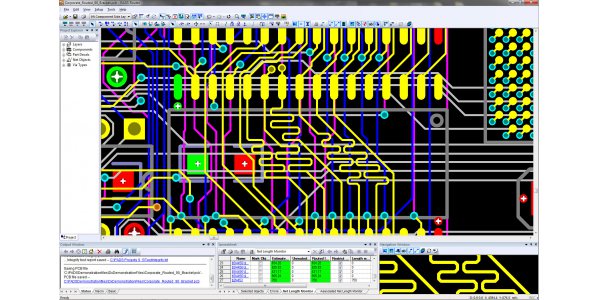
Pads is a computer software for designing, simulating electronic circuits and designing circuit boards. It was originally developed by Innoveda (Nasdaq:INOV), and then renamed Power PCB. In April 2002, Innoveda was acquired by Mentor Graphics (NASDAQ:MENT). Acquired and changed to the original name PADS again in recent years.
PADS is the mainstream PCB design platform in the industry. With its powerful interactive layout and easy-to-learn and easy-to-use features, PADS has been widely used in the most active industrial fields such as communications, semiconductors, consumer electronics, and medical electronics. PADS Layout/Router supports a complete PCB design process, covering import from schematic netlist, interactive layout and routing driven by rules, DRC/DFT/DFM verification and analysis, until the final production file (Gerber), assembly file And a full range of functional requirements such as bill of materials (BOM) output, to ensure that PCB engineers complete design tasks efficiently.
Ultiboard
- Full version: $ 2809.678
- Professional Edition:$ 4176
- Teaching class: $ 724.959
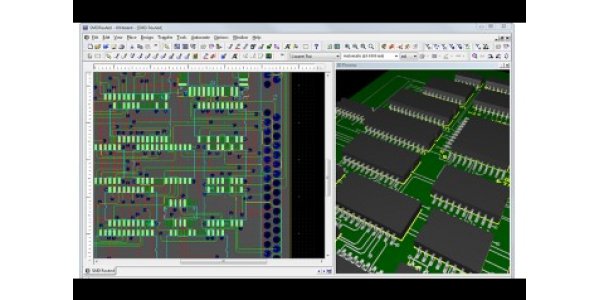
Multisim is a Windows-based simulation tool launched by National Instruments (NI) Co., Ltd., suitable for board-level analog/digital circuit board design. It includes graphical input of circuit schematics, circuit hardware description language input, and has rich simulation analysis capabilities.
Engineers can use Multisim to interactively build circuit schematics and simulate the circuit. Multisim refines the complex content of SPICE simulation so that engineers can quickly capture, simulate and analyze new designs without knowing in-depth SPICE technology, which also makes it more suitable for electronics education. Through Multisim and virtual instrument technology, PCB design engineers and electronics educators can complete a complete integrated design process from theory to schematic capture and simulation to prototype design and testing.
Provides a method of converting schematic diagrams and simulation data to other programs, and can output schematic diagrams to PCB wiring.
Altium Designer 20(Protel)

- $ 325 /Month
- $ 9990 /permanent
Altium Designer 20 represents decades of innovation and development dedicated to creating a truly unified design environment - one that enables users to effortlessly connect with every facet of the PCB design process.
Striking the perfect balance between power and ease of use, Altium Designer has secured its position as the most widely-used PCB design solution on the market.
The unified feature of Altium Designer allows design data to be seamlessly transferred from one design domain to the next. But first of all, the intuitively felt curve pattern of a large amount of data and information that is deeply expanded will show a huge obstacle to this productivity-enhancing environment and its rich functions. Therefore, the unique document core space of Altium Designer provides all the information needed to quickly start and run the software. From the high-level overview and step-by-step deployment, to the comprehensive coverage of all the fragmentary functions and information resources provided through the intuitive software interface, the Altium Designer documentation truly provides a readily available "knowledge tree" structure.
Features
Advanced wiring technology
Support trimming rigid-flex circuit board design
Powerful data management tools
The ECAD library contains more than 300,000 ready-to-use components
Powerful design reuse tool
Real-time cost estimation and tracking
Dynamic Supply Chain Intelligence
Native 3D visualization and gap inspection
Flexible release management tools
All these functions and the entire design process are implemented through a unified design environment (the only peer).
SOLIDWORKS PCB
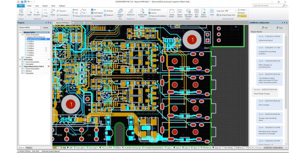
SOLIDWORKS PCB enables the productivity you need to design Printed Circuit Boards (PCBs) quickly along with unique, collaboration between electrical and 3D mechanical design teams. It offers a clear advantage where ECAD-MCAD collaboration is critical for overall success of electronic product design.
Function:
Rigid-Flex Design
Design and Data Management
ECAD-MCAD Design Collaboration
PCB Design Engine
Modern Schematic Entry
Streamlined Interface
Managed ECAD-MCAD ECO Process
Real-time 3D Clearance Checking
Mixed-Mode SPICE 3f5 Simulator
Supplier Links/Search
Version Control
Component Parametric Database Support
SOLIDWORKS File Support
Design Commenting and Revision Managemen
Kicad

KiCad (pronounced "Key-CAD") is a free software suite for electronic design automation (EDA). It facilitates the design of schematics for electronic circuits and their conversion to PCB designs. KiCad was originally developed by Jean-Pierre Charras. It features an integrated environment for schematic capture and PCB layout design. Tools exist within the package to create a bill of materials, artwork, Gerber files, and 3D views of the PCB and its components.
The KiCad suite has five main parts:
KiCad – the project manager.
Eeschema – the schematic capture editor.
Pcbnew – the PCB layout program. It also has a 3D view.
GerbView – the Gerber viewer.
Bitmap2Component – tool to convert images to footprints for PCB artwork.
Allegro PCB Designer
Key Benefits
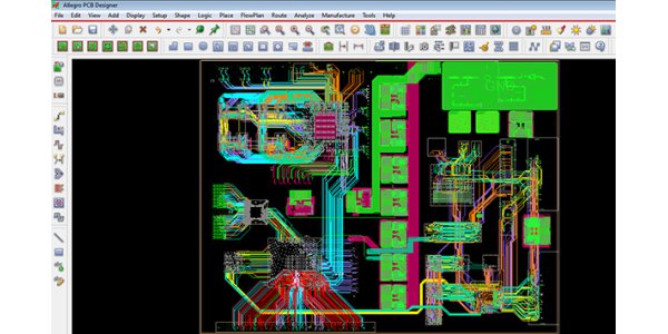
Speeds designs from placement and routing through to manufacturing
Includes powerful features such as design partitioning, RF design capabilities, and interconnect design planning
Production proven to increase productivity and help engineers quickly ramp up to volume production
TÜV SÜD “Fit for Purpose – TCL1” certified to meet ISO 26262 automotive functional safety requirements
Features
Provides a scalable, full-featured PCB design solution
Enables a constraint-driven design flow to reduce design iterations
Integrated DesignTrue DFM technology providing real-time DFM checks
Provides a single, consistent, front-to-back constraint management environment
Minimizes design iterations and lowers overall cost for flex and rigid-flex designs with advanced rigid-flex design capabilities
Enables dynamic concurrent team design capability to shorten design cycle by dramatically reducing time spent on routing, tuning, and optimization of signals
Delivers an integrated RF/analog design and mixed-signal design environment
Provides interactive floorplanning and component placement
Provides design partitioning for large, dispersed development teams
Enables real-time, interactive push/shove etch editing
Allows real-time plowing/healing with dynamic shape technology
Manages net scheduling, timing, crosstalk, layer set routing, and geometric constraints
Provides proven PCB router technology for auto-routing of random signals
Enables hierarchical route planning to accelerate design completion
Shortens interconnect planning and routing time for dense designs with high-speed interfaces
Provides a comprehensive, powerful, easy-to-use suite of tools to assist designers with an efficient and successful handoff to manufacturing:
DFM Checker for signoff against company/manufacturing-partner-specific rules
Documentation Editor for reducing fabrication and assembly documentation time up to 70%
Panel Editor for communicating assembly panel design intent to manufacturing partners
Outputs design data in a variety of manufacturing formats
Eagle

- $60/monthly
- $297/1 year
- $801/3 year
EAGLE is a scriptable electronic design automation (EDA) application with schematic capture, printed circuit board (PCB) layout, auto-router and computer-aided manufacturing (CAM) features. EAGLE stands for Easily Applicable Graphical Layout Editor (German: Einfach Anzuwendender Grafischer Layout-Editor) and is developed by CadSoft Computer GmbH. The company was acquired by Autodesk Inc. in 2016.
Orcad

OrCAD is a set of electronic design automation package software on personal computers, which is specially used for electronic engineers to design circuit diagrams and related diagrams, design printed diagrams for printed circuit boards, and circuit simulation.
ORCAD Capture (hereinafter referred to as Capture) is a circuit design tool based on Windows operating environment.
Using Capture software, it is possible to draw circuit schematics and provide continuous simulation information for the production of PCBs and programmable logic designs. As the industry standard PCB schematic input method, OrCAD Capture is one of the most popular schematic input tools in the world today, with a simple and intuitive user design interface. OrCAD Capture CIS has a powerful component information system that can manage component databases online and centrally, thereby greatly improving the efficiency of circuit design. OrCAD Capture provides a complete and adjustable schematic design method, which can be effectively applied to PCB design creation, management and reuse. Combining schematic design technology and PCB layout technology, OrCAD can help designers grasp the design intent from the beginning. Whether it is used to design analog circuits, complex PCBs, FPGAs and CPLDs, schematic modifications of PCB revisions, or to design hierarchical modules, OrCAD Capture can provide designers with fast design input tools. In addition, OrCAD Capture schematic input technology allows designers to input, modify and verify PCB designs at any time.
PADS (also known as Power PCB)

Pads is a computer software for designing, simulating electronic circuits and designing circuit boards. It was originally developed by Innoveda (Nasdaq:INOV), and then renamed Power PCB. In April 2002, Innoveda was acquired by Mentor Graphics (NASDAQ:MENT). Acquired and changed to the original name PADS again in recent years.
PADS is the mainstream PCB design platform in the industry. With its powerful interactive layout and easy-to-learn and easy-to-use features, PADS has been widely used in the most active industrial fields such as communications, semiconductors, consumer electronics, and medical electronics. PADS Layout/Router supports a complete PCB design process, covering import from schematic netlist, interactive layout and routing driven by rules, DRC/DFT/DFM verification and analysis, until the final production file (Gerber), assembly file And a full range of functional requirements such as bill of materials (BOM) output, to ensure that PCB engineers complete design tasks efficiently.
More resources:
Do you have any questions about the above-mentioned? Contact us now, we will reply to you soon.
Is the article useful to you?
No
Yes(
12
)
12
967
1
Share to:
