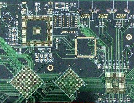
The ball grid array (BGA) is a type of surface-mount packaging (a chip carrier) used for integrated circuits. BGA packages are used to permanently mount devices such as microprocessors. A BGA can provide more interconnection pins than can be put on a dual in-line or flat package.
The whole bottom surface of the device can be used instead of just the perimeter. The traces connecting the package's leads to the wires or balls which connect the die to package are also on average shorter than with a perimeter-only type, leading to better performance at high speeds. Soldering of BGA devices requires precise control, and it is usually done by automated processes.
PBGA - - Stands for Plastic BGA. The carrier is a common printed board substrate. It is composed of two or four layers of organic materials. The chip is connected to the surface of the carrier by wire bonding. The surface of the plastic moulding carrier is connected with an eutectic solder ball array.
CBGA - - Stands for Ceramic BGA. The carrier is multi-layer ceramics. There are two forms of connection between chip and ceramic carrier: wire bonding and flip chip technology. It has the advantages of excellent electrical and thermal properties and good sealing.
CCBGA - - CCBGA is another form of CBGA when the size of CBGA is larger than 32*32mm. The difference is that solder column insteads of solder ball. The solder column is connected by eutectic solder or fixed at the bottom of the ceramics by direct casting.
According to the different packaging materials, BGA types are mainly as follows: PBGA (plastic BGA), CBGA (ceramic BGA), CCBGA (ceramic column BGA), TBGA (tape BGA).
TBGA - - The chip carrier uses bimetal layer tape, chip connection is realized by flip-chip technology. It fits lighter and smaller package, suitable for encapsulation with more I/O numbers. It also has good electrical performance, suitable for batch electronic assembly and high reliability of solder joint.
According to the production feedback of the board factory, it will often be mentioned that the via under the BGA is too close to the pad and the via needs to be moved. This situation is due to the fact that the vias are not equidistant from the BGA pads. Since the position of the vias and test holes under the BAG is not equidistant from the BGA pads, PCB designers do not pay attention to this, leading to continuous engineering problems, so cause hidden danger to welding quality. Therefore, we directly recommend punching to the center of the two pads, especially because the pitch of the PGA is small in the BGA. After punching, it is necessary to cover the via plug hole under the BGA to avoid short circuit of the BGA ball and tin.