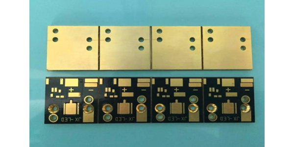
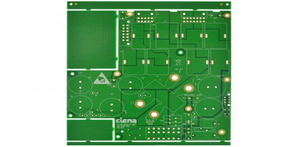
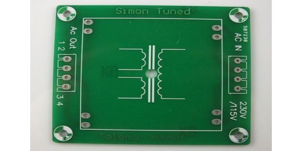
The so-called copper cladding is based on free PCB space and then filled with solid copper, also known as copper fill. The important significance of copper coating is to reduce the grounding impedance, improve the anti-interference ability, reduce the pressure drop, improve the power supply efficiency, and connect with the ground wire, reduce the loop area. If the PCB has more pads, Sgnd, Agnd, GND, etc., how to cover the copper? My approach is to use the most important "base" as a reference for the individual copper separately depending on the location of the PCB, separating the digital and analog to apply the copper from many words. At the same time in the copper cladding, the first bolded corresponding power connection: v5.0v, v3.6v, v3.3v, etc. As a result, many different shapes of polymorphic structures are formed.
1): one is a different single point connection, practice is through 0 ohm resistance or magnetic bead or inductance connection.
2): the second is the crystal near the copper cladding. The circuit of crystal vibration is the high-frequency transmitting source. In practice, the copper is applied around the crystal, and then the crystal vibration of the shell is grounded in other ways.
3): if the feeling is very large, then the definition of a hole is not much. In addition, the large area of copper is good or mesh clad copper is good, large area of copper cladding, if through wave soldering, the plate may tilt upward, or even blisters. From this Angle.

Copper clad PCB basic handling method:
Generally, there are two basic ways of covering copper, that is, covering a large area of copper and copper mesh. Large area of copper coating, with increased current and shielding double effect, but large area of copper coating, if the wave soldering, the board may be up, and even bubble. Therefore, large area of copper, generally will also open a few slots, ease the bubble of copper foil. Simple grid copper coating or shielding function, increase the role of the current is reduced, from the point of view of heat dissipation, the grid is good (it reduces the heating surface of copper) and played a certain role of electromagnetic shielding. But it should be pointed out that, the grid is composed of alternating direction go line, we know for circuit line width for the work frequency of the circuit board has its corresponding "electricity" length of (actual size divided by the working frequency of the corresponding digital frequency, concrete books), when the working frequency is not high, perhaps is not very obvious, the side effects of grid lines once electrical length and working frequency matching, is very bad, you will find that the circuit won't work properly, emission signal interference system work everywhere. So for those of you who use a grid, my advice is to choose based on how well the circuit board is working, and not to cling to one thing at a time. Therefore, the high frequency circuit against interference requirements of the multi-purpose grid, low frequency circuit, circuit with large current, etc., commonly used complete copper.

A thick copper PCB, including several pieces of cascading set of core board, one of the most outer layer of the two pieces of core board outside set with copper foil, copper foil and between core board, core board and core board between the first half has curing, core board including thick copper layer, each side has its core thickness of copper layer is adjacent to the second half of the curing, described in the second half of curing on a chip with the corresponding thickness of copper layer graphics instead of gong to take, described in the copper foil and core board described by more than the first half cure piece, the second half cure bonding connection.
Copper clad PCB manufacturing process:
The thick copper PCB, near the location of the core thickness of copper layer is set in the second half, curing and curing in the second half on a chip is equipped with corresponding graphics instead of gong to bring thick copper layer, namely gong PP lamination design, core board after pressing large filling adhesive thickness without copper area to: thickness of copper thick - pressing gong PP theory, core board with no copper resin filling was increased greatly, which can effectively solve bigger without copper thick copper PCB area factors bring underfill resin flow in the process of pressing the pressing hole and the thickness of inequalities.
1). Further, core board includes dielectric layer, the dielectric layers is described with either one or both described in the thick layer of copper, the thickness of copper layer effective graphic area is larger and closed position of copper thick copper area, mentioned in the second half piece of corresponding curing thick copper the location of gong gong cavity formation, empty the same second half curing bulge formed between adjacent gong cavity, the thickness of copper layer thick copper area formed between adjacent sag, described in the thick copper layer of concave and convex of the adjacent second half curing one-to-one correspondence nested pressing.
2). Further, the adjacent first half solidified sheet and the second half solidified sheet are integrated into one forming structure.
3). Further, the first half of the adjacent curing sheet and the second half of the curing sheet are of split structure, which are connected together when pressed.
4). Further, between the copper foil and the core plate, and between the core plate and the core plate, there are many pieces of the first half of the curing sheet.
5). Further, the thickness of the thick copper layer is ≥4oz.
6). Further, the thick copper PCB comprises four laminated core plates, and the thick copper layer is arranged on both sides of the medium layer of the core plate.

The existence of copper clad PCB:
With the rapid development of the electronic information age, the demand for high-power, high-current PCB such as the server power board is increasing, and these power boards need high heat resistance, high heat dissipation and other characteristics, prefer the design of thick copper plate; Thick copper plate because of the thick thick copper (4 oz) or higher characteristic, in PCB machining production process there are many difficulties, especially in the pressing process, the traditional producing method, larger without copper area appear easily after pressing the pressing hole, the problem of uneven thickness, of graphic design, selection and matching of pressing the PP and the rise of temperature of the compressor and vacuum capacity have larger limit.
