1). The calculation method is as follows:
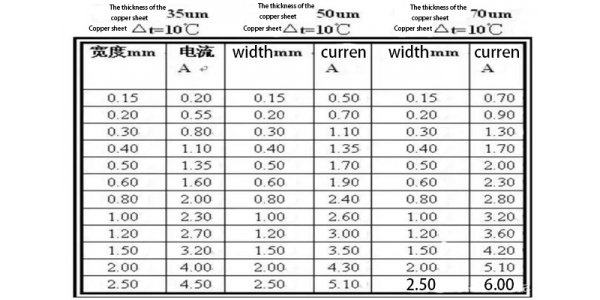
First, the cross-sectional area of Track is calculated. The thickness of copper foil of most PCB is 35um (if you are not sure, you can ask the PCB manufacturer, the thickness of 1 ounce is 35um, which is actually less than 35um).
There is an empirical value of current density of 15 to 25 amperes per square millimeter. If you weigh the upper cross-sectional area you get the flux capacity. I=KT0.44A0.75 (K is the correction coefficient, 0.024 for the inner layer of copper clad wire, and 0.048T for the maximum temperature rise in the outer layer. The unit is Celsius (the melting point of copper is 1060℃). A is the copper clad cross section area, and the unit is square MIL(not mm mm, note is square MIL.)I is the maximum allowable current
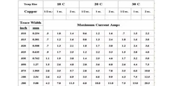
The calculation of PCB current carrying capacity is always short of authoritative technical methods and formulas, and experienced CAD engineers can make accurate judgments based on their personal experience. But for the CAD novice, it is not a problem. The current carrying capacity of PCB depends on the following reasons: wire width, wire thickness (copper foil thickness), allowable temperature rise. As we all know, the wider the PCB goes, the greater the current carrying capacity. Here, please tell me: assuming that under the same conditions, a 10MIL wire can withstand 1A, then how much current can a 50MIL wire withstand? Is it 5A? The answer, of course, is no. Please see the following data provided by international authorities: line width is in units of Inch (Inch in =25.4 millimillimm) 1 oz. Copper =35 micron thick, 2 oz.=70 micron thick, 1 oz =0.035mm 1mil.=10-3 inch.trace Carrying Capacity per mil STD 275
In the experiment, the voltage drop caused by the wire resistance caused by the length of the wire must be considered. The tin on process welding is only to increase the current capacity, but it is difficult to control the volume of tin. 1 OZ copper, 1mm wide, generally 1-3 A galvanometer, specific to your line length, pressure drop requirements.
The maximum current value should be the maximum allowable value under the temperature rise limit. The fuse value is the value at which the temperature rise reaches the melting point of copper. Eg. 50mil 1oz temperature rise 1060 degrees (i.e. copper melting point), current is 22.8A.

2.The main reason that affects the carrying value of the line current:
1). The bearing value listed in the table data is the maximum bearing value of the current at room temperature of 25 degrees, so it is necessary to consider all kinds of environment, manufacturing process, plate process, plate quality and other reasons in the actual planning. So the table provides only as a reference value.
2). In the actual planning, each conductor is also affected by the welding plate and the hole, such as solder taught many line segments, after the tin, solder that its current carrying value will be greatly increased, many people may have seen some big current board between welding plate and welding plate in a certain section of the line was destroyed, the reason is very simple, after the bonding pad for a tin because of components and soldering enhance its current carrying value, the wires and solder and solder pad between its maximum current carrying value is to allow the largest current carrying conductor width values. Moment fluctuation of the circuit, therefore, it is easy to burn out that a line between welding plate and welding plate, fix: adding wire width, such as plate must not be allowed to increase wire width, add a layer of Solder the wires layer (typically 0.6 1 mm wires can increase a layer of Solder wire around, of course you also add a 1 mm layer of Solder wire) after a tin, so this article 1 mm wires can be regard as a 1.5 mm ~ 2 mm wire (depending on the homogeneous degree of the conductor is a tin tin and tin).
3. The relationship between copper foil thickness, wire width and current during PCB planning:
The current strength of the signal. When the average current of the signal is large, the current that the wiring width can bear should be considered. The wire width can refer to the following data:
1). The relationship between copper foil thickness, wire width and current during PCB planning;
2). The carrying capacity of copper foil with different thickness and width is shown in the following table:

4.Empirical formula:
I = KT0.44 A0.75
(K is the correction coefficient. For general copper clad wire, the maximum temperature rise is 0.024 in the inner layer and 0.048t in the outer layer, the unit is Celsius (the melting point of copper is 1060℃).
A is the copper clad cross-sectional area in square MIL(not mm mm, but square MIL);
I is the maximum allowable current and the unit is amp.
Generally, 10mil=0.010inch=0.254 can be 1A,250MIL=6.35mm, or 8.3A.
5.PCB calculation formula:
Firstly, the cross-sectional area of track is calculated. The copper foil thickness of most PCB is 35um (if you are not sure, you can ask the PCB manufacturer). The cross-sectional area is multiplied by the width of the line. There is an empirical value of current density of 15 to 25 amperes per square millimeter. If you weigh the upper cross-sectional area you get the flux capacity.
6.PCB design rules:
PCB design rules and constraints are very useful functions of PCB design software. There are physical constraints on PCB layout and wiring, such as line width, line spacing, hole size, etc., as well as signal constraints, such as network impedance, crosstalk, signal reflection and wiring length. PCB design rule constraints can be broadly classified as: electrical constraints, wiring constraints, layout constraints, SMT table binding constraints, SI constraints, manufacturing constraints, high-speed setting constraints, and so on.
