PCB, full name printed circuit board, is a kind of circuit board made in a similar printing way. In fact, it turns the actual cable with different lengths into the metal wire of resin board, greatly reducing the use of wire, saving space and energy consumption.
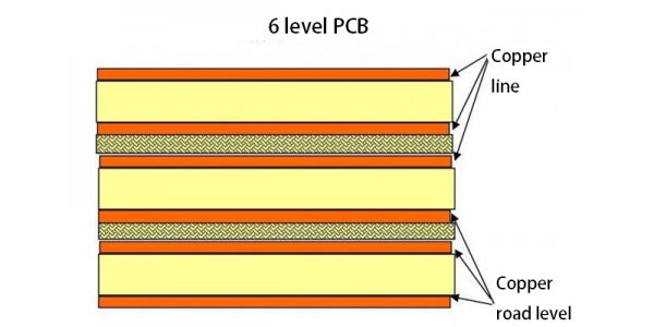
PCB is a kind of printed circuit board, so the common PCB is several layers glued together, each layer has resin insulation substrate and metal circuit layer.
The biggest difference between multilayer PCB and single panel or double panel is that the internal power layer (keep the internal power layer) and ground layer are added. The power and ground network are mainly wired on the power layer. However, the multilayer board wiring is mainly based on the top layer and the bottom layer, supplemented by the middle wiring layer. Therefore, the design method of multilayer board is basically the same as that of double-sided board. The key lies in how to optimize the wiring of internal electric layer, so that the wiring of circuit board is more reasonable and the electromagnetic compatibility is better.

Generally speaking, four layers can meet the normal operation of PCB, so the so-called six layers, eight layers and ten layers are actually adding more circuit layers to improve the electrical capacity of PCB, that is, the pressure bearing capacity. Therefore, the increase of PCB layers means that more circuits can be designed inside.
Characteristics of Hybrid Multilayer PCB:
The biggest difference between multilayer PCB and single panel or double panel is that the internal power layer (keep the internal power layer) and ground layer are added. The power and ground network are mainly wired on the power layer. However, the multilayer board wiring is mainly based on the top layer and the bottom layer, supplemented by the middle wiring layer. Therefore, the design method of multilayer board is basically the same as that of double-sided board. The key lies in how to optimize the wiring of internal electric layer, so that the wiring of circuit board is more reasonable and the electromagnetic compatibility is better.
With the continuous development of SMT (surface mount technology) and the continuous introduction of new generation SMD (surface mount devices), such as QFP, QFN, CSP, BGA (especially MBGA), electronic products are more intelligent and miniaturized, thus promoting the major reform and further progress of PCB industry technology.
The biggest difference between multilayer PCB and single panel or double panel is that the internal power layer (keep the internal power layer) and ground layer are added. The power and ground network are mainly wired on the power layer. However, the multilayer pcb wiring is mainly based on the top layer and the bottom layer, supplemented by the middle wiring layer. Therefore, the design method of multilayer board is basically the same as that of double-sided board. The key lies in how to optimize the wiring of internal electric layer, so that the wiring of circuit board is more reasonable and the electromagnetic compatibility is better.
No matter what the internal quality of multilayer pcb is, we can see the differences through the surface. These differences are very important for the durability and functionality of PCB during its whole life. The following are the important features of high reliability multilayer pcb:
1. The copper thickness of the hole wall of multilayer pcb is 25 μ m, which has the advantages of enhanced reliability, including improved z-axis expansion resistance. But there are also certain risks: under the actual use, the problems of electrical connectivity (inner layer separation, hole wall fracture) or the possibility of failure under the load condition in the process of blowing out or degassing, assembly. IPC class2 (the standard of most factories) requires PCB multilayer board to be copper plated less than 20%.

2. No welding repair or open circuit repair advantages: perfect circuit ensures reliability and safety, no maintenance and no risk. Disadvantages: if the maintenance is improper, the PCB multilayer board is open. Even if fixed properly, there may be risk of failure under load conditions (vibration, etc.), which may lead to failure in actual use.
3. Advantages beyond the cleanliness requirements of IPC specification: improving the cleanliness of PCB multilayer can improve the reliability. Risk: the residue on the terminal block, the accumulation of solder will take the risk of welding mask, and the ion residue will lead to the risk of corrosion and pollution on the welding surface, which may lead to reliability problems (poor solder joint / electrical failure) and eventually increase the probability of actual failure.
4. Strictly control the service life advantages of each surface treatment: the risks of welding, reliability and water intrusion are unfinished. The risks are that the surface treatment of old PCB multilayer plate may cause metallographic changes, while the water intrusion may cause problems and / or actual use of delamination in the assembly process, separation (open circuit) of inner wall and wall wall, etc.
The advantages of Hybrid Multilayer PCBs include:
• small size: one of the most prominent and acclaimed benefits of using mixed multilayer PCBs is their size. Because of its layered design, multilayer PCB itself is smaller than other PCBs with similar functions. This has brought huge benefits to modern electronics, as the current trend is to focus on smaller, more compact but more powerful gadgets such as smartphones, laptops, tablets and wearable devices.
• lightweight structure: smaller PCB, lighter weight, especially because multiple connectors required for interconnection of single and double PCB are cancelled, which is conducive to multilayer design. Once again, it's good for modern electronics, which tend to be more mobile.
• high quality: these types of PCBs tend to be better than single-layer and double-layer PCBs when making multilayer PCBs due to a lot of work and planning. As a result, they are also more reliable.
• improve durability: multilayer PCBs are often durable due to their nature. These multilayer PCBs must not only bear their own weight, but also be able to handle the heat and pressure used to glue them together. In addition to these factors, multilayer PCBs use multilayer insulation between circuit layers, combining them with prepreg adhesives and protective materials.
• increased flexibility: Although this does not apply to all multilayer PCB components, some do use flexible construction techniques to form flexible multilayer PCBs. This may be an ideal feature for applications where slight bending and bending may occur on a semi regular basis. Similarly, this does not apply to all multilayer PCBs, and the more layers are added to the flexible PCB, the less flexible the PCB is.
More powerful function: the mixed multilayer PCB is a very high density component, which combines multilayer into one PCB. These close-up make circuit boards more connected, and their inherent electrical performance enables them to achieve greater capacity and speed, albeit in smaller sizes.
• single connection point: hybrid multilayer PCBs are designed to be used as a single unit rather than in series with other PCB components. As a result, they have a single connection point, rather than multiple connection points required to use multiple single-layer PCBs. This proves to be useful in electronic product design as they only need to include a single connection point in the final product. This is particularly useful for small electronics and gadgets designed to minimize size and weight.
These advantages make multilayer PCB very useful in various applications, especially in mobile devices and high-function electronic devices. In turn, as many industries turn to mobile solutions, hybrid multilayer PCBs occupy a place in more and more industry-specific applications.
